Manufacturing process of electrode surface protective layer of multilayer piezoelectric element

A piezoelectric element and electrode surface technology, applied in the direction of electrical components, piezoelectric/electrostrictive/magnetostrictive devices, circuits, etc., can solve the problems of reducing product yield, component damage, affecting product quality, etc., to achieve guaranteed The effect of low yield, low bending rigidity, and small added mass

Active Publication Date: 2011-10-05
AUDIOWELL ELECTRONICS GUANGDONG
View PDF8 Cites 5 Cited by
  • Summary
  • Abstract
  • Description
  • Claims
  • Application Information

AI Technical Summary

Problems solved by technology

In this solution, since the curing temperature of the protective material is different from the sintering temperature of the piezoelectric film, the coating or printing of the protective layer must be carried out after the sintering of the piezoelectric film is completed, and then curing or secondary sintering is performed, and the process is relatively complicated.
The complexity of the process is mainly manifested in two aspects: one is the high rigidity and poor toughness of the multilayer piezoelectric element, which may cause damage to the element during the printing process of the protective layer and reduce the yield of the product
Second, piezoelectric ceramic materials are very sensitive to temperature, high temperature curing or secondary sintering will affect the performance of piezoelectric elements, thus affecting the quality of products

Method used


Image

  • Manufacturing process of electrode surface protective layer of multilayer piezoelectric element
  • Manufacturing process of electrode surface protective layer of multilayer piezoelectric element

Examples


Embodiment Construction

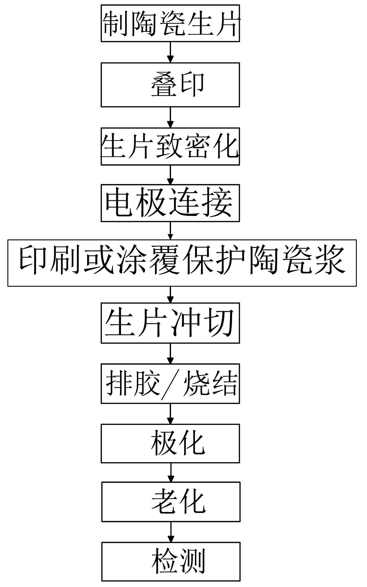
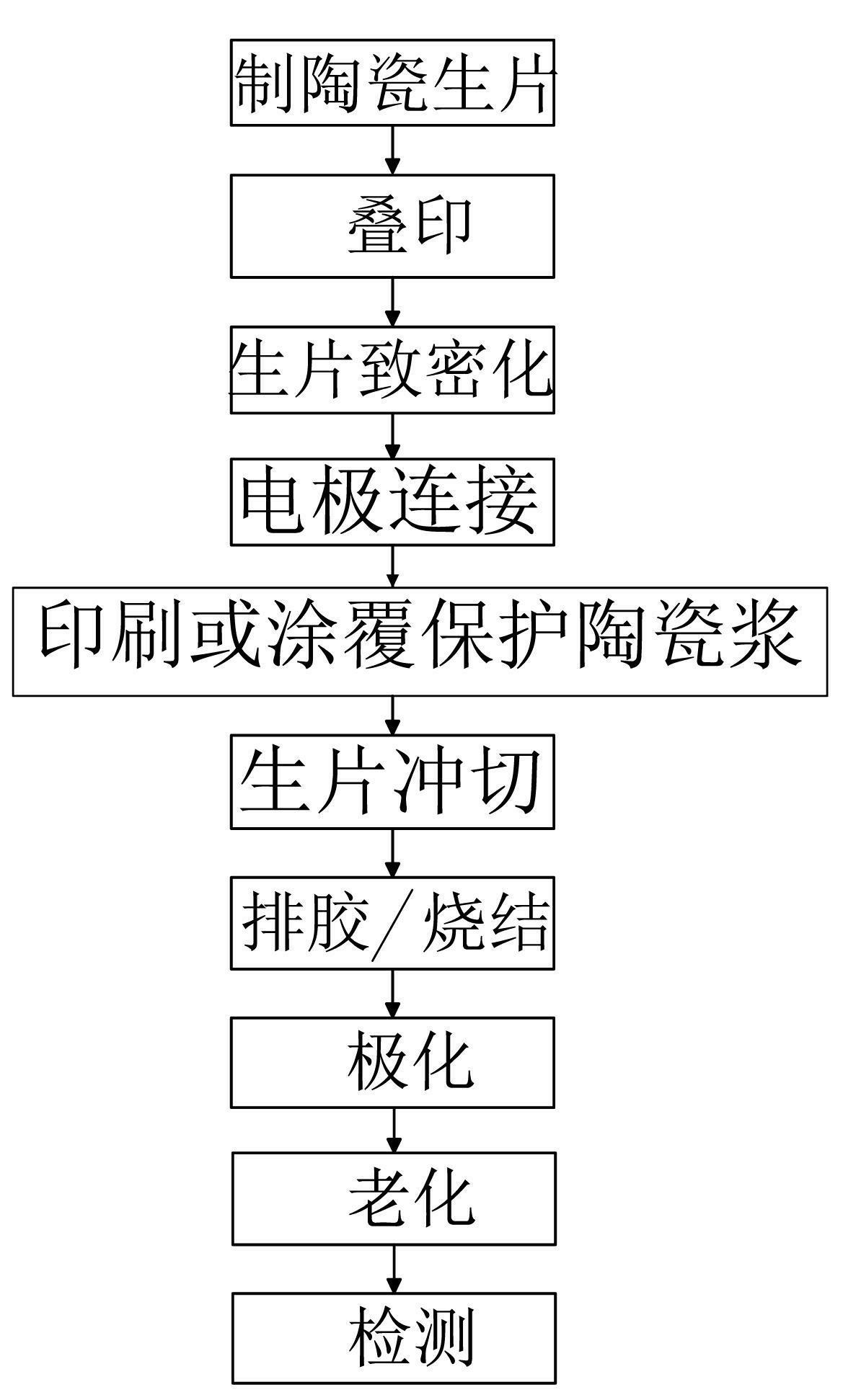
[0018] refer to figure 1 , a typical fabrication process flow diagram of a multilayer piezoelectric element, which includes the following steps:

[0019] 1. Making ceramic green sheets: making ceramic green sheets by casting or other processes;

[0020] 2. Overprinting: printing electrode paste on the surface of the ceramic green sheet to form an electrode layer, and superimposing the ceramic green sheet with the printed electrode layer layer by layer to form a multi-layer structure;

[0021] 3. Densification of green sheets: Under certain temperature and pressure conditions, the multi-layer green sheets are integrated into one, which is the densification of green sheets;

[0022] 4. Electrode connection: The interlayer electrode connection is completed by various known methods. In this step, the internal electrode connection can be performed after the slicing is completed, or the internal electrode connection can be performed after sintering;

[0023] 5. Printing or coating...


PUM

PropertyMeasurementUnit
thicknessaaaaaaaaaa

Abstract

The invention provides a manufacturing process of an electrode surface protective layer of a multilayer piezoelectric element. In the preparation of the multilayer piezoelectric element, ceramic slurry is printed or coated on a raw ceramic sheet where a surface electrode of an unsintered multi-layer structure is in, and then the multi-layer structure is sintered to be integrally molded, wherein the unsintered multi-layer structure is formed by overlapping the raw ceramic sheet, an interlayer electrode and the surface electrode. Because the sintering temperature of the ceramic slurry is close to those of the ceramic raw sheet and the electrode slurry, a ceramic protective film can be integrally formed on the surface electrode of the multilayer piezoelectric element by using the method provided by the invention and the thickness of the ceramic protective film can be controlled according to a printing or coating technique so that a protective layer with an extremely small thickness can be obtained; the protective film generates small additional mass, has a very small effect on the bending rigidity of the element and provides effective insulating protection to the surface electrode ofthe multilayer piezoelectric element without affecting the property of the element; and the protective film is applicable to various piezoelectric elements for different purposes and is also definitely applicable to single-layer piezoelectric elements.

Description

technical field [0001] The invention relates to a manufacturing process of an electrode surface protection layer in a piezoelectric element, in particular to a manufacturing process of a multilayer piezoelectric element surface layer electrode surface protection layer. Background technique [0002] Compared with single-layer piezoelectric elements, multilayer piezoelectric elements can obtain greater bending or linear deformation with a smaller voltage, so they are widely used in piezoelectric motors, piezoelectric actuators, piezoelectric transformers, piezoelectric Speakers and other piezoelectric devices are an important piezoelectric element. For multilayer piezoelectric transducer elements, in addition to the formulation and sintering process of piezoelectric materials and electrode pastes, the electrode insulation protection of multilayer piezoelectric elements is an important aspect that determines the performance of piezoelectric elements. At present, for multilayer...

Claims


Application Information

Patent Timeline
Patent Type & Authority Applications(China)
IPC IPC(8): H01L41/24H01L41/273
Inventor 姜德星秦小勇苗洛祥郑涛
Owner AUDIOWELL ELECTRONICS GUANGDONG
Why Eureka
Try Eureka