Preparation method of LDMOS (Laterally Diffused Metal Oxide Semiconductor) for efficiently collecting substrate current

A technology of substrate current and active area, which is used in circuits, electrical components, semiconductor/solid-state device manufacturing, etc.

Inactive Publication Date: 2011-10-19
SHANGHAI INTEGRATED CIRCUIT RES & DEV CENT
View PDF3 Cites 15 Cited by
  • Summary
  • Abstract
  • Description
  • Claims
  • Application Information

AI Technical Summary

Problems solved by technology

like figure 1 and figure 2 As shown, in a traditional LDMOS structure, the active region includes a source region 9, a drain region 8, and a body lead-out region 11, and the body lead-out region 11 and the source region 9 are separated by a field region 2, and in the N-type drift region 5 A drain region 8 is formed, an active region 9 and a body lead-out region 11 are formed in the P-type body region 7, and the formation process is as follows: performing P in the P-type body region 7 + injection, forming P + The doped region is used as the body lead-out region 11, and the N-type drift region 5 and the P-type body region 7 are respectively carried out. + Implantation forms N-type doped regions, which are respectively used as drain region 8 and source region 9; gate region 3 is formed on the substrate, and channel implantation is performed on gate region 3 to form a channel region under gate region 3 (not marked in the figure), wherein a contact hole 13 is formed on the source region 9, the drain region 8, the gate region 3, the N-type drift region 5, and the P-type body region 7, since the source region 9 is located at the body lead out 11 Between the channel region below the gate region 3, the source region 9 is separated from the body lead-out region 11 to the middle of the channel region, so the body lead-out region 11 is far away from the channel region, resulting in redundant lining in the channel region. The bottom current cannot be collected through the body lead-out region 11 in time

Method used


Image

  • Preparation method of LDMOS (Laterally Diffused Metal Oxide Semiconductor) for efficiently collecting substrate current
  • Preparation method of LDMOS (Laterally Diffused Metal Oxide Semiconductor) for efficiently collecting substrate current
  • Preparation method of LDMOS (Laterally Diffused Metal Oxide Semiconductor) for efficiently collecting substrate current

Examples


Embodiment Construction

[0024] In order to make the content of the present invention clearer and easier to understand, the content of the present invention will be further described below in conjunction with the accompanying drawings of the specification. Of course, the present invention is not limited to this specific embodiment, and general replacements well known to those skilled in the art are also covered by the protection scope of the present invention.

[0025] Secondly, the present invention uses schematic diagrams to describe in detail. When describing the examples of the present invention, for convenience of explanation, the schematic diagrams are not partially enlarged according to the general scale and should not be used as a limitation to the present invention.

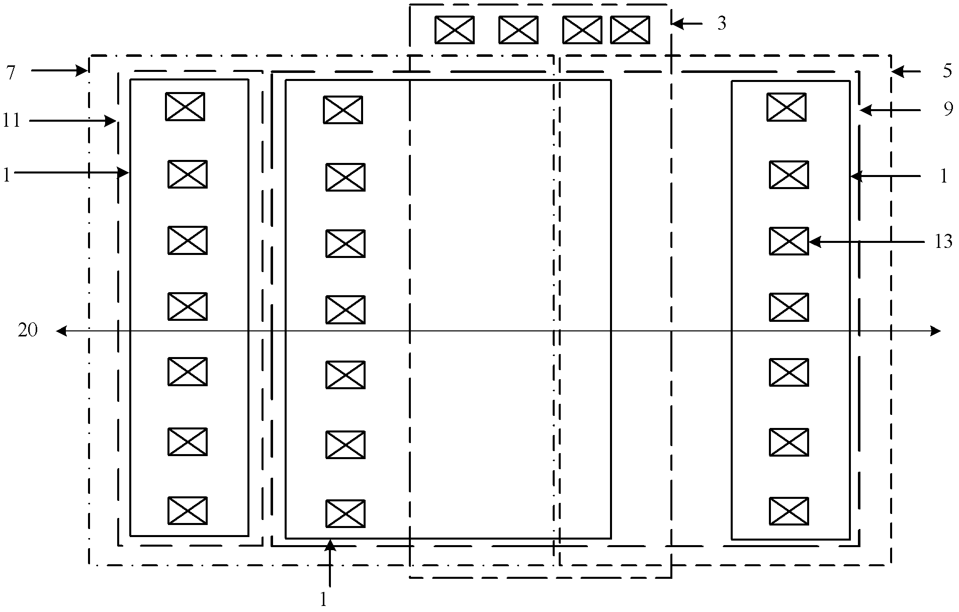
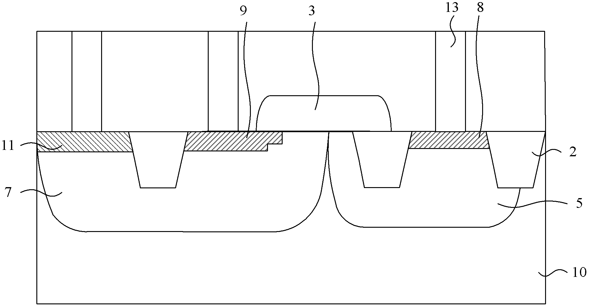
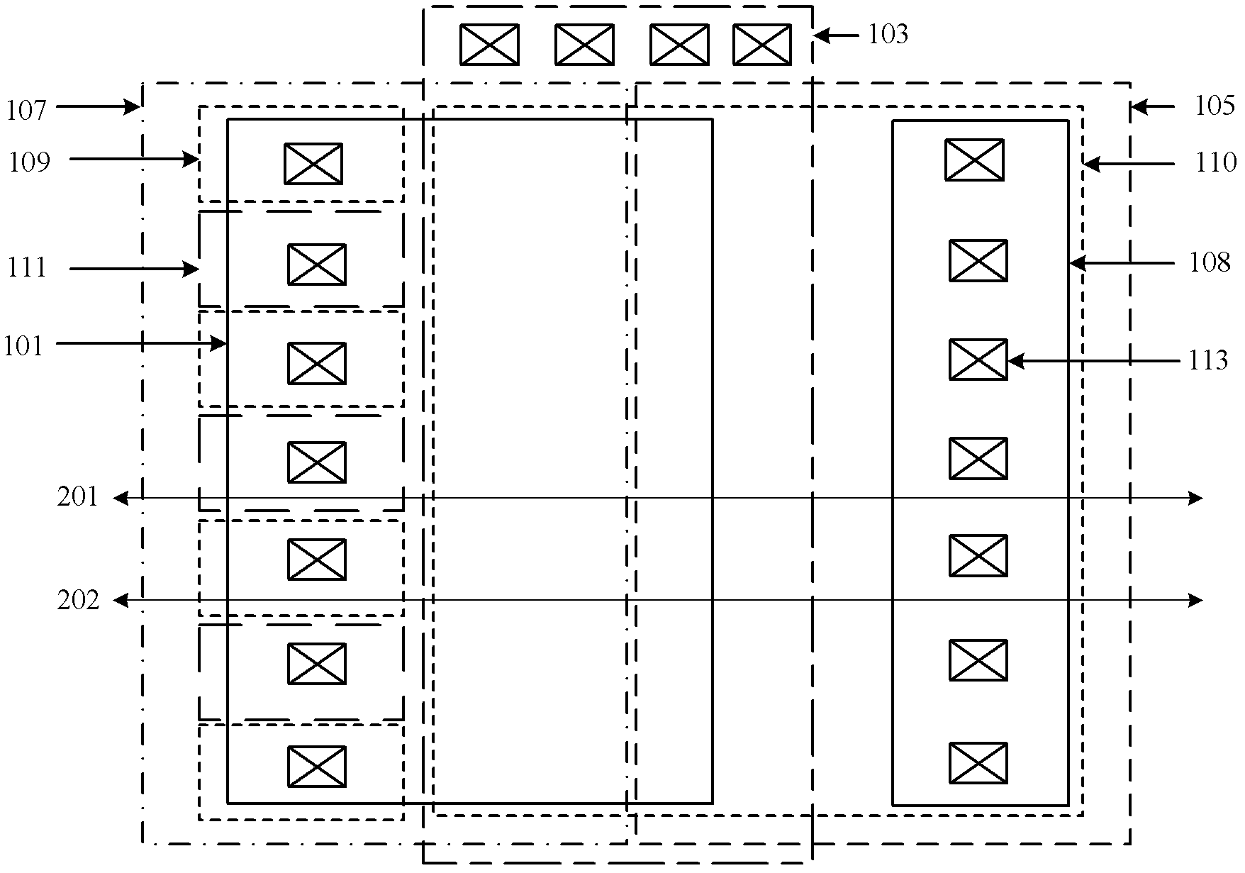
[0026] The present invention aims to provide a method for preparing LDMOS that effectively collects substrate current, and by using the N + Injection version and P + The implanted plate is implanted into the source, drain and body reg...


PUM


Abstract

The invention discloses an LDMOS (Laterally Diffused Metal Oxide Semiconductor) preparation method for efficiently collecting substrate current, wherein the method comprises the following steps: adopting standard preparation technology of LDMOS, and realizing the LSMOS capable of efficiently collecting the substrate current just through the following layout design, namely, using an active region, an N-type drift region and a P-type body region to form the drain region, the source region and the body leading-out region of an LDMOS device; defining a channel region by using polycrystalline; and realizing the drain electrode, the source electrode and the body leading-out electrode by using N+ injection and P+ injection. The regions used for source electrode leading-out N+ injection and the regions used for body leading-out P+ injection are arranged alternatively in the source region. In the invention, the body leading-out position is closer to the channel region formed by a hot carrier and the corresponding substrate current; therefore, the substrate current can be more efficiently collected, parasitical NPN (Negative-Positive-Negative) bipolar transistor is prevented from being turned on due to overlarge substrate current, the device is prevented from entering Snapback state for burning, and the purpose of enlarging safe work area of the LDMOS is achieved.

Description

Technical field [0001] The invention relates to a preparation method of LDMOS in a semiconductor device, in particular to a preparation method of LDMOS which can effectively collect substrate current. Background technique [0002] In display drive and power management products, we need to provide high-voltage devices that can withstand high voltages and pass large currents. High-voltage LDMOS is often used in high-voltage power integrated circuits to meet the requirements of high-voltage resistance and power control. LDMOS (Lateral Diffusion Metal Oxide Semiconductor Device) is widely used because it is more compatible with CMOS technology. We can get high-performance LDMOS devices with only a small amount of changes to the CMOS process. [0003] LDMOS devices are usually used for high-voltage switches. When LDMOS is switching, its voltage on the drain and gate regions reaches the maximum at the same time. Under the action of strong electric field and large current, impact ioniza...

Claims


Application Information

Patent Timeline
Patent Type & Authority Applications(China)
IPC IPC(8): H01L21/336
Inventor 顾学强肖慧敏王言虹
Owner SHANGHAI INTEGRATED CIRCUIT RES & DEV CENT
Why Eureka
Try Eureka