Conductive optical element, touch panel, information input device, display device, solar cell, and master for production of conductive optical element

A technology of optical components and master plates, applied in optical components, electrical components, optics, etc., can solve problems such as increased reflection, reduced transmittance of transparent conductive film, and deterioration of display device quality, achieving improved productivity and good anti-reflection performance , The effect of improving the transmission characteristics

Inactive Publication Date: 2011-10-19
DEXERIALS CORP
View PDF5 Cites 10 Cited by
  • Summary
  • Abstract
  • Description
  • Claims
  • Application Information

AI Technical Summary

Problems solved by technology

However, if the thickness of the transparent conductive layer formed of a high-refractive index material increases, the reflection of external light at the interface between the transparent conductive layer and the substrate increases, so that the transmittance of the transparent conductive film decreases
Therefore, there is a problem that the quality of the display device may deteriorate

Method used


Image

  • Conductive optical element, touch panel, information input device, display device, solar cell, and master for production of conductive optical element
  • Conductive optical element, touch panel, information input device, display device, solar cell, and master for production of conductive optical element
  • Conductive optical element, touch panel, information input device, display device, solar cell, and master for production of conductive optical element

Examples


no. 3 approach

[0125] 3. The third embodiment (the example of the two-dimensional configuration of the structure into an arc and another hexagonal lattice shape: refer to Figure 18 )

[0126] 4. The fourth embodiment (an example in which the structure is arranged in a meandering manner: refer to Figure 21 )

[0127] 5. The fifth embodiment (an example of forming a concave structure on the surface of a substrate: refer to Figure 22 )

[0128] 6. Sixth Embodiment (Example of S-shaped Refractive Index Distribution: Refer to Figure 26 )

[0129] 7. Seventh Embodiment (Example of Forming Structures on Both Main Surfaces of a Conductive Optical Element: Refer to Figure 29 )

[0130] 8. Eighth Embodiment (Example of Forming a Structure by Thermal Transfer: Refer to Figure 30 )

[0131] 9. Ninth Embodiment (example applied to a resistive touch panel: refer to Figure 31 A and Figure 31 B)

[0132] 10. Tenth Embodiment (Example of forming a hard coat layer on the touch surface of a ...

no. 1 approach

[0144] [Structure of Conductive Optical Element]

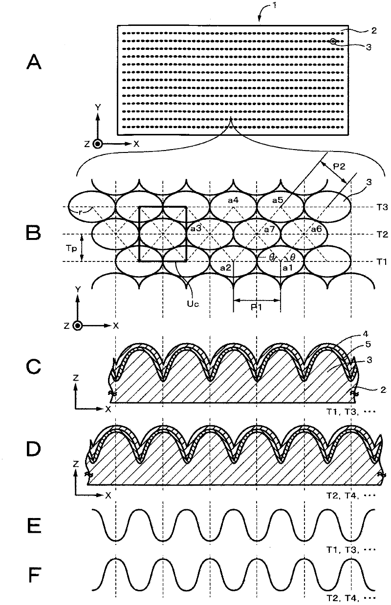
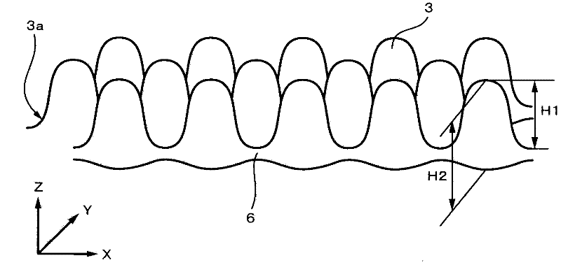
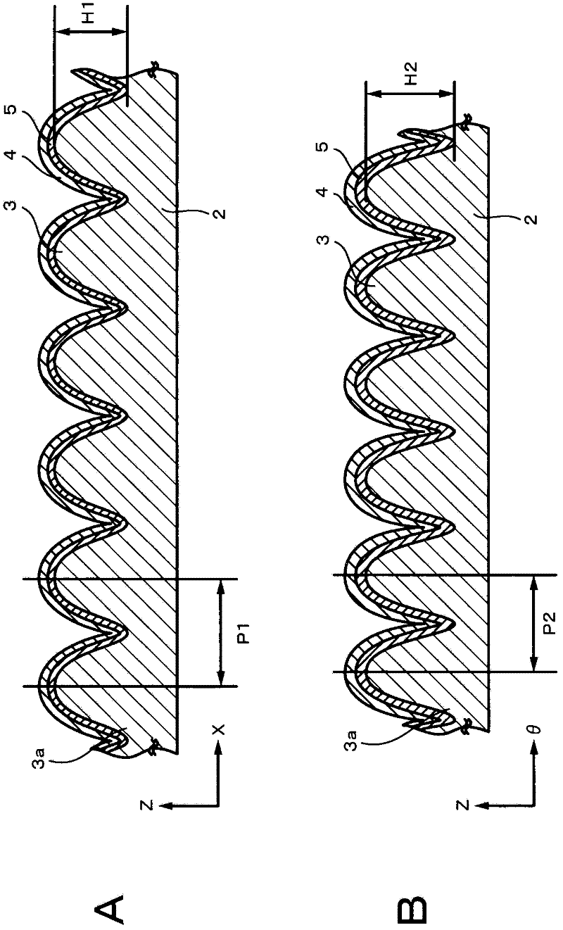
[0145] figure 1 A is a schematic plan view showing a configuration example of the conductive optical element according to the first embodiment of the present invention. figure 1 B is shown figure 1 A partially enlarged plan view of the conductive optical element shown in A. figure 1 C is along figure 1 Cross-sectional views taken from traces T1, T3, . . . shown in B. figure 1 D is along figure 1 Cross-sectional views taken from traces T2, T4, . . . shown in B. figure 1 E is shown in the form corresponding to figure 1 B shows a schematic diagram of the modulation waveform of the laser light used for the latent images of the trajectories T1, T3, . . . figure 1 F is shown in the form corresponding to figure 1 B shows a schematic diagram of the modulation waveform of the laser light used for the latent images of the trajectories T2, T4, . . . figure 2 as well as Figure 4 to Figure 6 are shown figure 1 A shows a partia...

no. 2 approach

[0245] [Structure of Conductive Optical Element]

[0246] Figure 15 A is a schematic plan view showing a configuration example of a conductive optical element according to a second embodiment of the present invention. Figure 15 B is shown Figure 15 A partially enlarged plan view of the conductive optical element shown in A. Figure 15 C is along Figure 15 Cross-sectional views taken from traces T1, T3, . . . shown in B. Figure 15 D is along Figure 15 Cross-sectional views taken from traces T2, T4, . . . shown in B. Figure 15 E is shown in the form corresponding to Figure 15 B shows a schematic diagram of the modulation waveform of the laser light used for the latent images of the trajectories T1, T3, . . . Figure 15 F is shown in the form corresponding to Figure 15 B shows a schematic diagram of the modulation waveform of the laser light used for the latent images of the trajectories T2, T4, . . .

[0247] The conductive optical element 1 according to the se...


PUM

PropertyMeasurementUnit
thicknessaaaaaaaaaa
thicknessaaaaaaaaaa
electrical resistivityaaaaaaaaaa

Abstract

Disclosed is a conductive optical element which comprises: a base having a surface; a structure composed of a plurality of conical projections or recesses that are arranged on the surface of the base at a fine pitch that is not more than the wavelength of visible light; and a transparent conductive film formed on the structure. The aspect ratio of the structure is 0.2-1.3 (inclusive), and the transparent conductive film has a surface following the shape of the structure. The average film thickness (Dm1) of the transparent conductive film at the tops of the structure is not more than 80 nm, and the surface resistivity of the transparent conductive film is within the range of 50-50 (inclusive).

Description

technical field [0001] The present invention relates to a conductive optical element, a touch panel, an information input device, a display device, a solar cell, and a master for manufacturing the conductive optical element. Specifically, the present invention relates to a conductive optical element provided with a transparent conductive film on one main surface of a base thereof. Background technique [0002] In recent years, resistive touch panels for inputting information have been provided on display devices such as liquid crystal display elements included in mobile devices and cellular phone devices. [0003] The resistive touch panel has a structure in which two transparent conductive films are disposed opposite with respect to a space formed of an insulating material such as acrylic resin therebetween. The transparent conductive film is used as an electrode of the touch panel and includes a substrate having transparency (for example, a polymer film) and a high refrac...

Claims


Application Information

Patent Timeline
Patent Type & Authority Applications(China)
IPC IPC(8): G02B1/11B32B3/30G02B1/10G06F3/041G06F3/045H01B5/14
CPCB32B3/30G02B1/11G02B5/0231G06F3/042G06F3/0428H01L31/022466H01L31/022475H01L31/0236Y02E10/50G06F3/045H01B5/14
Inventor 梶谷俊一林部和弥村本穣远藤惣铭木村清广竹之内正树
Owner DEXERIALS CORP
Why Eureka
Try Eureka