Antireflective double layer P/N heterojunction graded composite material with monocrystalline silicon as carrier, and application thereof

A composite material and monocrystalline silicon technology, which is applied in organic compound/hydride/coordination complex catalysts, chemical/physical processes, physical/chemical process catalysts, etc., can solve the problems of low photoelectric conversion efficiency, difficulty in recycling, and easy agglomeration and other problems, to achieve the effect of low reaction equipment requirements, reduced recombination, and mild conditions

Active Publication Date: 2016-06-08
JIANGNAN UNIV
View PDF6 Cites 4 Cited by
  • Summary
  • Abstract
  • Description
  • Claims
  • Application Information

AI Technical Summary

Problems solved by technology

[0004] The purpose of the present invention is to overcome the shortcomings of traditional titanium dioxide/polypyrrole composites such as disorder, easy agglomeration, difficult recovery and low photoelectric conversion efficiency, and provide an anti-reflective double-layer P/N heterogeneous composite

Method used


Image

  • Antireflective double layer P/N heterojunction graded composite material with monocrystalline silicon as carrier, and application thereof
  • Antireflective double layer P/N heterojunction graded composite material with monocrystalline silicon as carrier, and application thereof
  • Antireflective double layer P/N heterojunction graded composite material with monocrystalline silicon as carrier, and application thereof

Examples


Embodiment 1

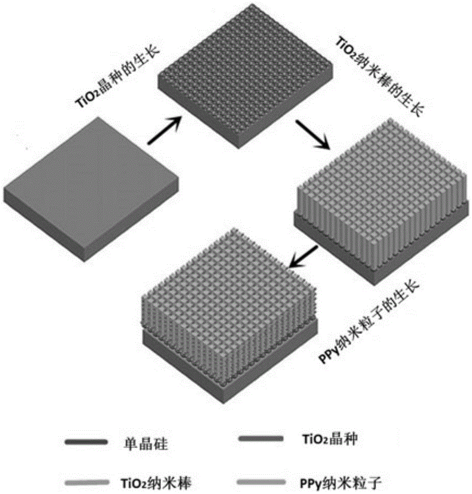
[0024] Step 1: Growth of TiO on the surface of single crystal silicon 2 seed crystal

[0025] Place the wafer in NH 3 h 2 O, H 2 o 2 and H 2 In the mixed solution of O, the volume ratio is 1:1:5, the temperature is 80°C, and the heating time is 30min. Then, immerse in the isopropanol solution of tetrabutyl titanate with a concentration of 0.075mol / L for pulling. The pulling speed is 2mm / s, and the pulling is repeated 20 times. Finally, the above sample is placed in a 450°C muffle Calcined in the furnace for about 30min.

[0026] Step 2: TiO 2 Seed induced TiO 2 Preparation of nanorods

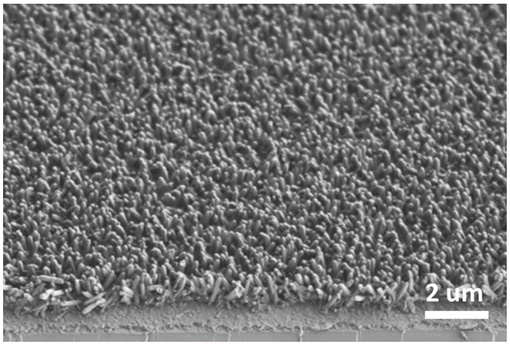
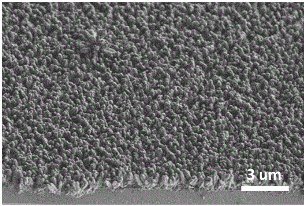
[0027] Attach TiO to the surface obtained in step 2 2 The seeded silicon wafers were placed under hydrothermal conditions to grow TiO 2 Nano stave. The hydrothermal synthesis condition is at a temperature of 130°C, and treated in a reaction kettle filled with 10mL deionized water, 10mL concentrated hydrochloric acid (37% by mass fraction) and 0.5mL tetrabutyl titanate for 8h, and th...

Embodiment 2

[0032] Step 1: Growth of TiO on the surface of single crystal silicon 2 seed crystal

[0033] Place the wafer in NH 3 h 2 O, H 2 o 2 and H 2 In the mixed solution of O, the volume ratio is 1:1:5, the temperature is 80°C, and the heating time is 40min. Then, immerse in the isopropanol solution of tetrabutyl titanate with a concentration of 0.05mol / L for pulling. The pulling speed is 2mm / s, and the pulling is repeated 15 times. Finally, the above sample is placed in a 450°C muffle Calcined in the furnace for about 1h.

[0034] Step 2: TiO 2 Seed induced TiO 2 Preparation of nanorods

[0035] The surface obtained in step 1 is attached with TiO 2 The seeded silicon wafers were placed under hydrothermal conditions to grow TiO 2 Nano stave. The hydrothermal synthesis condition is at a temperature of 130°C, and treated in a reactor filled with 10mL deionized water, 10mL concentrated hydrochloric acid (37% mass fraction) and 0.5mL tetrabutyl titanate for 8h, and then the s...

Embodiment 3

[0040] Step 1: Growth of TiO on the surface of single crystal silicon 2 seed crystal

[0041] Place the wafer in NH 3 h 2 O, H 2 o 2 and H 2 In the mixed solution of O, the volume ratio is 1:1:5, the temperature is 90°C, and the heating time is 30min. Then, immerse in the isopropanol solution of tetrabutyl titanate with a concentration of 0.1mol / L for pulling. The pulling speed is 2mm / s, and the pulling is repeated 10 times. Finally, the above sample is placed in a 500°C muffle Calcined in the furnace for about 30min.

[0042] Step 2: TiO 2 Seed induced TiO 2 Preparation of nanorods

[0043] The surface obtained in step 1 is attached with TiO 2 The seeded silicon wafers were placed under hydrothermal conditions to grow TiO 2 Nano stave. The hydrothermal synthesis condition is at a temperature of 120°C, and treated in a reactor filled with 10mL of deionized water, 10mL of concentrated hydrochloric acid (37% by mass) and 0.5mL of tetrabutyl titanate for 8h, and then ...


PUM

PropertyMeasurementUnit
Particle sizeaaaaaaaaaa
The average particle sizeaaaaaaaaaa
The average diameteraaaaaaaaaa

Abstract

The invention relates to an antireflective double layer P/N heterojunction graded composite material with monocrystalline silicon as a carrier. A preparation method of the composite material comprises the following steps: 1, carrying out hydrophilic treatment on a silicon chip, growing titanium dioxide seeds on the growth of the hydrophilically treated silicon chip, and calcining the obtained silicon chip in a muffle furnace; 2, placing the silicon chip with the surface attached with the titanium dioxide seeds, obtained in step 1, in a reaction kettle, and inducing growth of titanium dioxide nano-rods on the surface of the silicon chip through a hydrothermal synthesis technology; and 3, depositing the titanium dioxide nano-rods on polypyrrole nano-particles obtained in step 2 to obtain the antireflective double layer P/N heterojunction graded composite material with monocrystalline silicon as a carrier. The antireflective double layer P/N heterojunction graded composite material with monocrystalline silicon as a carrier has excellent material surface light reflection reduction and efficient photo-induced charge separation ability, and can be applied in the fields of photocatalysis, photoelectric conversion devices and solar batteries.

Description

technical field [0001] The invention relates to a layered composite material of an anti-reflective double-layer P / N heterojunction with monocrystalline silicon as a carrier, that is, a silicon-titanium dioxide-polypyrrole composite material. At the same time, this composite material can be used for photoelectric conversion and photocatalytic materials. It belongs to the technical field of photoelectric materials. Background technique [0002] At present, inorganic semiconductor photocatalysts such as TiO 2 , ZnO, MnO 2 , V 2 o 5 , Fe 3 o 4 ,, Ag 2 O etc. have been widely used in the field of renewable energy and environmental treatment. Among them, titanium dioxide nanomaterials have the advantages of high catalytic activity, good stability, fast degradation speed, mild degradation conditions, low investment, low energy consumption, high yield of hydroxyl radicals, and no corrosion under light. Sterilization and other aspects have shown particularly prominent applica...

Claims


Application Information

Patent Timeline
IPC IPC(8): B01J31/38A62D3/17A62D101/28
CPCA62D3/17A62D2101/28B01J21/063B01J31/06B01J31/38B01J35/0006
Inventor 石刚李赢王大伟倪才华何飞迟力峰吕男
Owner JIANGNAN UNIV
Why Eureka
Try Eureka