Light-emitting diode package structure manufacturing method

A technology of light-emitting diodes and packaging structures, which is applied to electrical components, circuits, semiconductor devices, etc., and can solve the problems of high material costs and process costs

Active Publication Date: 2011-11-02
INST OF SEMICONDUCTORS - CHINESE ACAD OF SCI
View PDF18 Cites 17 Cited by
  • Summary
  • Abstract
  • Description
  • Claims
  • Application Information

AI Technical Summary

Problems solved by technology

Some chip-scale light-emitting diode packages (ASE Semiconductor Manufacturing Co., Ltd. ZL200610108560.4, China Taiwan Epistar Co., Ltd. US20100163907A1) have

Method used


Image

  • Light-emitting diode package structure manufacturing method
  • Light-emitting diode package structure manufacturing method

Examples


Embodiment Construction

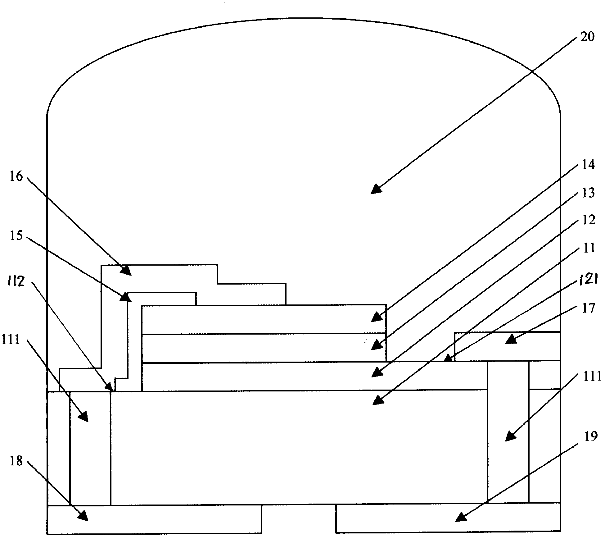
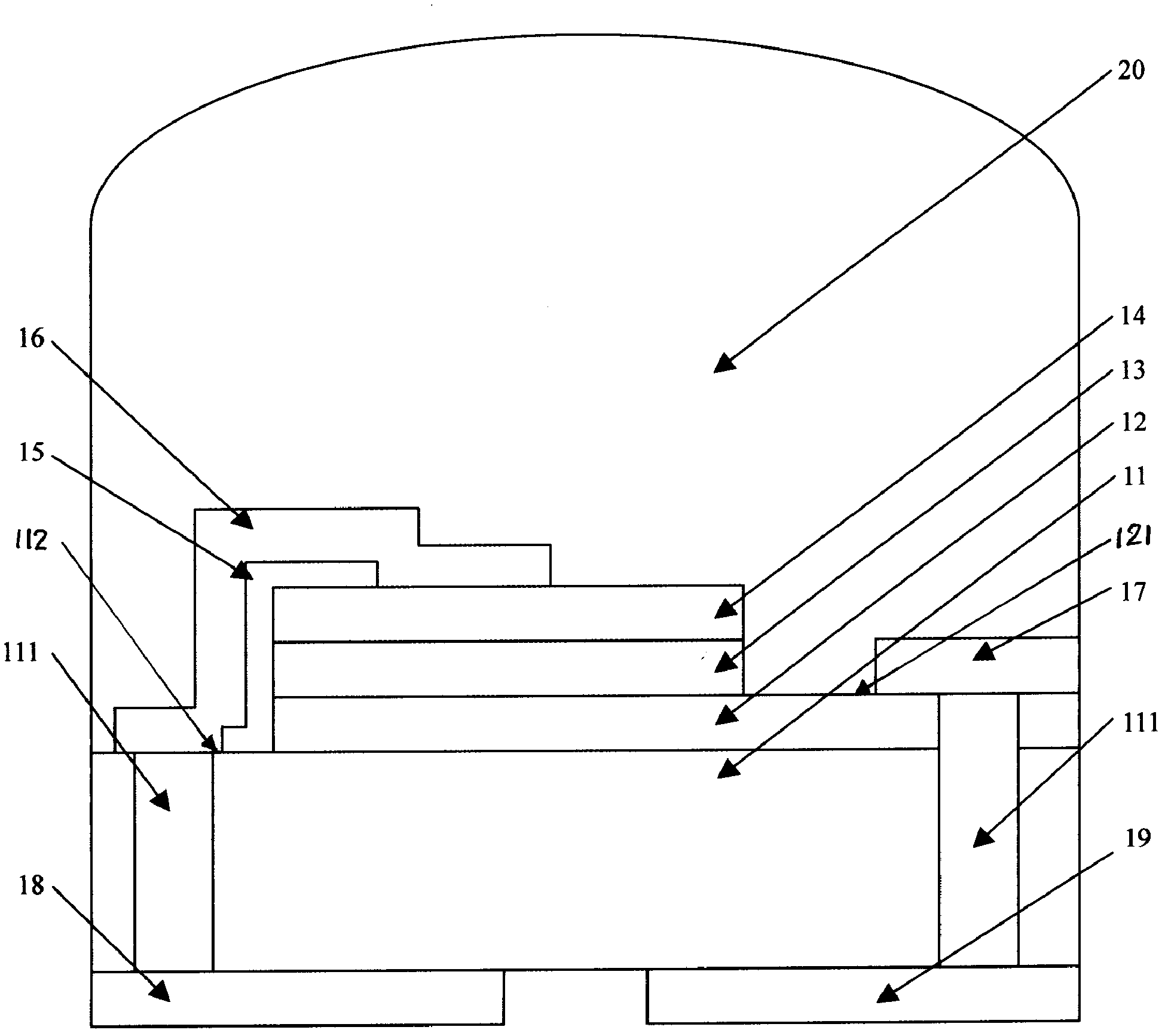
[0026] see figure 1 As shown, the present invention provides a method for manufacturing a light emitting diode packaging structure, comprising the following steps:

[0027] On an insulating substrate 11, the n-type layer 12, the active layer 13 and the p-type layer 14 are sequentially grown by metal-organic vapor phase epitaxy to form an epitaxial layer; wherein the material of the insulating substrate 11 is sapphire or silicon carbide or nitride Aluminum; wherein the n-type layer 12 and the p-type layer 14 in the epitaxial structure are upright or reversed. The material of the n-type layer 12 is n-type GaN, the material of the active layer 13 is a quantum well structure made of GaN material, and the material of the p-type layer 14 is p-type GaN.

[0028] The side above the p-type layer 14 is etched downward by a photolithography process, and the etching depth reaches the surface of the n-type layer 12 to form a first mesa 121, and the other side above the p-type layer 14 is ...


PUM


Abstract

The invention discloses a light-emitting diode package structure manufacturing method, which comprises the following steps of: sequentially growing an n-type layer, an active layer and a p-type layer on an insulating substrate by utilizing a metal organic vapor phase epitaxial method; downwards photoetching one side of the upper surface of the p-type layer with the photoetching depth of reaching the surface of the n-type layer to form a first tabletop, downwards etching the other side with the etching depth of reaching the surface of the insulating substrate to form a second tabletop; manufacturing conductive through holes on the first and second tabletops, and filling conductive metals; manufacturing an insulating layer partially covering the upper surface of the p-type layer on the sideclose to the second tabletop; manufacturing a p electrode covering the insulating layer on the insulating layer; manufacturing an n electrode on the conductive through hole on the first tabletop; thinning the insulating substrate; manufacturing a first back electrode and a second back electrode on the two sides of the back of the insulating substrate to form a substrate of a device; packaging an optical element on the substrate of the device to finish manufacturing the device on the substrate; and cutting the device on the substrate into independent devices in a mechanical way.

Description

technical field [0001] The invention belongs to the technical field of semiconductors, and in particular refers to a method for preparing a light-emitting diode packaging structure by using a wafer-level in-situ packaging technology. Background technique [0002] At present, the preparation process of light-emitting diodes is generally divided into three main steps: material epitaxy, chip technology, and chip packaging. The basic function of semiconductor device packaging is to connect micro-sized chip electrodes to relatively large-sized electrode structures for practical use. [0003] The LED packaging process generally uses some kind of substrate, case or bracket, and the LED chip is bonded to the substrate, case or bracket in some way, and then the electrodes on the upper part of the chip are connected to each other through the gold wire ball bonding process. To the corresponding electrodes on the substrate, case or bracket to achieve electrical connection, and finally ...

Claims


Application Information

Patent Timeline
IPC IPC(8): H01L33/00H01L33/48H01L33/38
Inventor 杨华卢鹏志谢海忠于飞郑怀文薛斌伊晓燕王军喜王国宏李晋闽
Owner INST OF SEMICONDUCTORS - CHINESE ACAD OF SCI
Why Eureka
Try Eureka