Macrolattice mismatch epitaxial buffer layer structure containing digital dislocation separating layers and preparation method thereof

A technology of isolation layer and buffer layer, applied in the direction of final product manufacturing, sustainable manufacturing/processing, electrical components, etc., can solve the problems of small and complex bandgap width, achieve low cost, simple preparation method, and good application prospects Effect

Inactive Publication Date: 2011-11-23
SHANGHAI INST OF MICROSYSTEM & INFORMATION TECH CHINESE ACAD OF SCI
View PDF5 Cites 7 Cited by
  • Summary
  • Abstract
  • Description
  • Claims
  • Application Information

AI Technical Summary

Problems solved by technology

[0005] The technical problem to be solved by the present invention is to provide a large lattice mismatch epitaxial material buffer layer structure containing a digital alloy dislocation isolation layer and its preparation method. The material contains a digital alloy dislocation isolation layer, which can make the large lattice The matching epitaxial material relaxes quickly and effectively in the buffer layer to release the stress, and isolates the threading dislocations, thereby reducing the threading dislocation density of the epitaxial material on the buffer layer and improving the efficiency of the large lattice mismatch epitaxial material on the buffer layer. Excellent lattice quality and photoelectric properties, and overcome the shortcomings of traditional strain-compensated superlattice dislocation isolation layers with small bandgap width and complicated parameter adjustment

Method used


Image

  • Macrolattice mismatch epitaxial buffer layer structure containing digital dislocation separating layers and preparation method thereof
  • Macrolattice mismatch epitaxial buffer layer structure containing digital dislocation separating layers and preparation method thereof
  • Macrolattice mismatch epitaxial buffer layer structure containing digital dislocation separating layers and preparation method thereof

Examples


Embodiment 1

[0024] For epitaxy of In on InP substrates 0.8 Ga 0.2 Buffer Layer Structure Containing InGaAs Digital Alloy Dislocation Isolation Layer of As Large Lattice Mismatch Material

[0025] (1) It is high-quality In with a thicker epitaxial thickness on the InP substrate .8 Ga 0.2 As large lattice mismatch material, it needs to be in the epitaxial In .8 Ga 0.2 The buffer layer was grown before the As material;

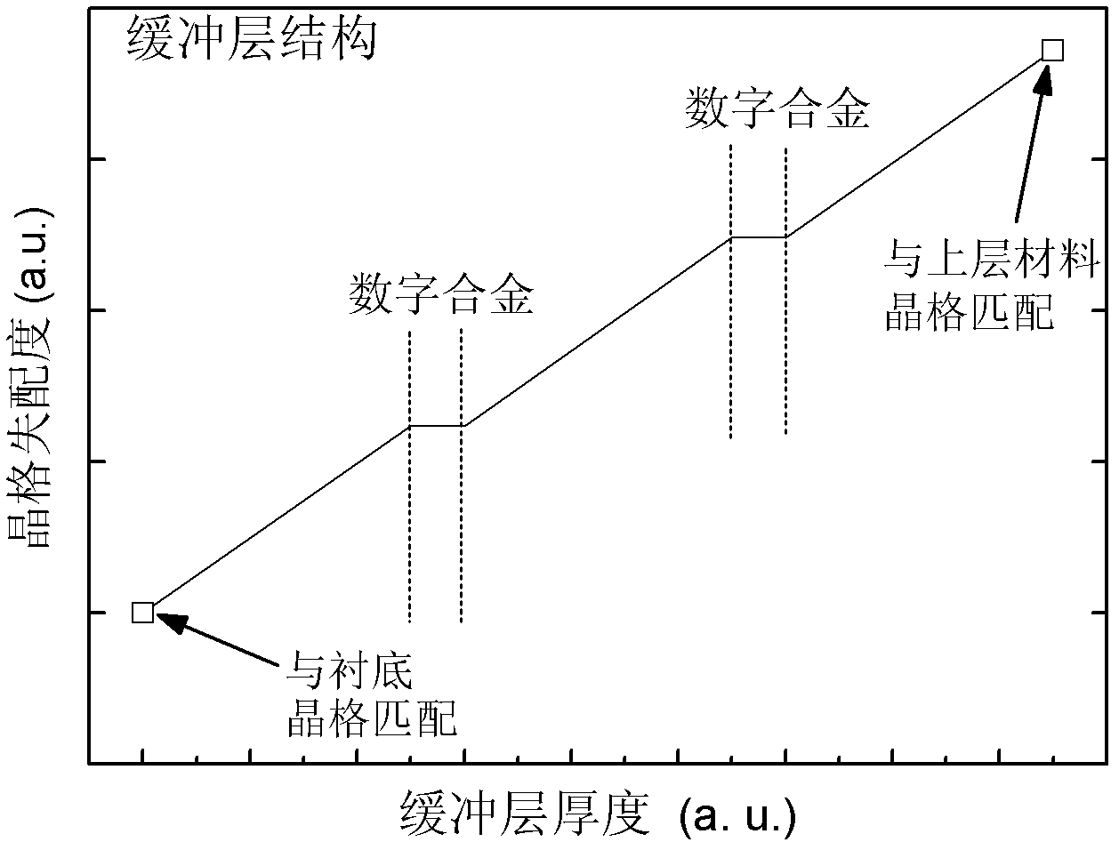
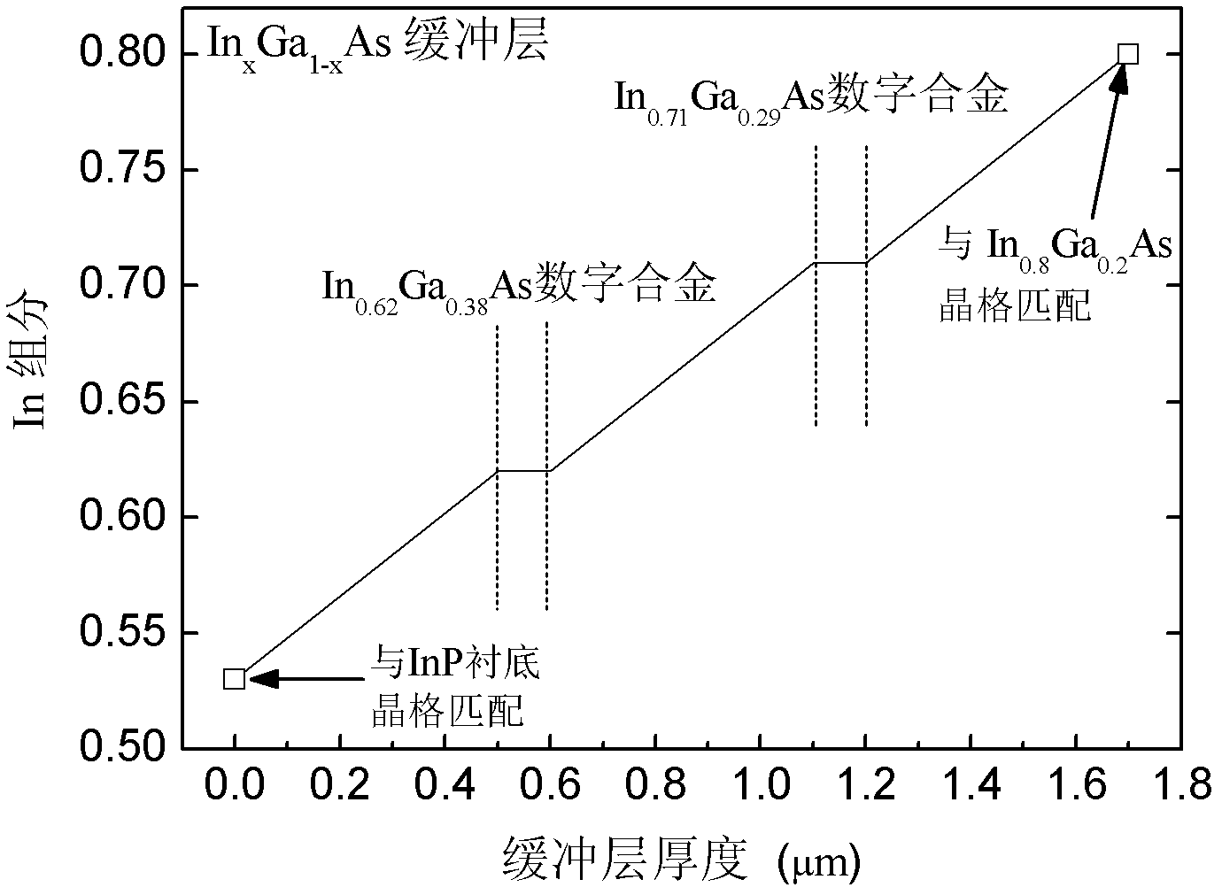
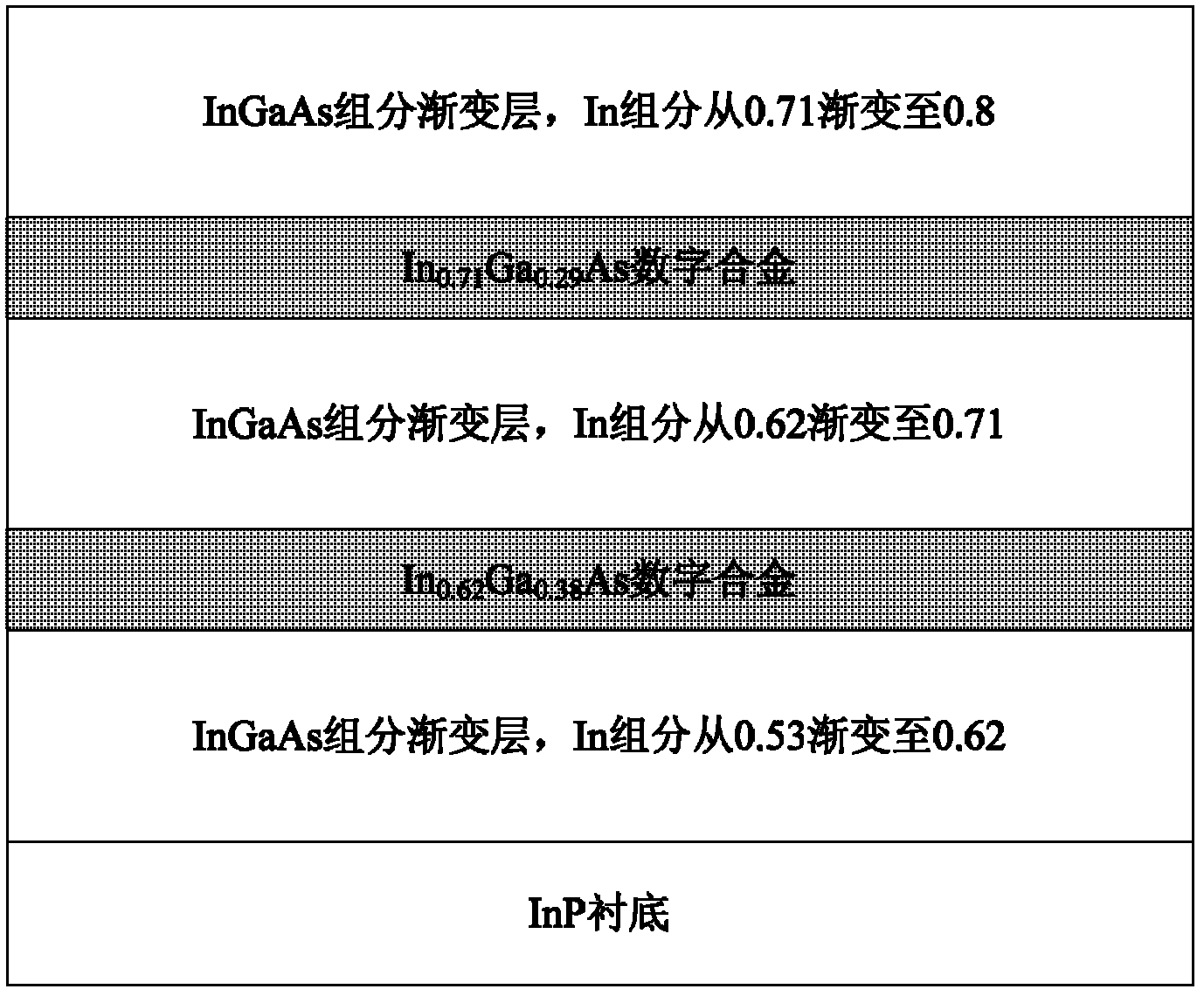
[0026] (2) The conventional molecular beam epitaxy method is used to grow the material, and the schematic diagram of the In composition change in the buffer layer structure is as follows figure 2 As shown, the schematic diagram of the buffer layer structure is shown in image 3 shown in the In x Ga 1-x Two layers of InGaAs digital alloys are inserted into the As composition gradient buffer layer, and the buffer layer is divided into 3 parts on average;

[0027] (3) The growth process of the buffer layer structure is composed of InP lattice-matched InP substrate 0....

Embodiment 2

[0034] For epitaxy of In on GaAs substrates 0.3 Al 0.7 Buffer Layer Structure Containing InAlAs Digital Alloy Dislocation Isolation Layer of As Large Lattice Mismatch Material

[0035] (1) High-quality In with thicker epitaxial thickness on GaAs substrate .3 Al 0.7 As large lattice mismatch material, it needs to be in the epitaxial In .3 Al 0.7 The buffer layer was grown before the As material;

[0036] (2) The conventional molecular beam epitaxy method is used to grow the material, and the schematic diagram of the In composition change in the buffer layer structure is as follows Figure 4 As shown, the schematic diagram of the buffer layer structure is shown in Figure 5 shown in the In x Al 1-x Two layers of InAlAs digital alloys are inserted into the As composition gradient buffer layer, and the buffer layer is divided into 3 parts on average;

[0037] (3) The growth process of the buffer layer structure starts with the growth parameters of the AlAs material lattic...


PUM

PropertyMeasurementUnit
Thicknessaaaaaaaaaa
Thicknessaaaaaaaaaa

Abstract

The invention relates to a macrolattice mismatch epitaxial buffer layer structure containing digital dislocation separating layers and a preparation method thereof. The structure is characterized in that n layers of digital alloy dislocation separating layer materials are inserted into an ingredient gradual changing buffer layer. The preparation method comprise the following steps: adjusting beam source temperature, growing a ingredient gradual changing buffer layer on a substrate, and according to present gradual changing ingredient, forming a digital alloy dislocation separating layer through growing short period superlattice; adjusting the beam source temperature again, growing a ingredient gradual changing buffer layer, regrowing a digital alloy dislocation separating layer according to present gradual changing ingredient; regrowing a ingredient gradual changing buffer layer in above sequence until the buffer layer ingredient gradually changes to a desirable value to obtain the macrolattice mismatch epitaxial buffer layer structure. According to the invention, the macrolattice mismatch epitaxial material takes place relaxation and releases stress rapidly and effectively in the buffer layer and isolates penetrating dislocation, thus penetrating dislocation density of the epitaxial material on the buffer layer is reduced, and crystal lattice quality and photoelectric characteristic of the macrolattice mismatch epitaxial material on the buffer layer are improved.

Description

technical field [0001] The invention belongs to the field of large lattice mismatch epitaxy materials and preparation thereof, in particular to a large lattice mismatch epitaxy material buffer layer structure containing a digital alloy dislocation isolation layer and a preparation method thereof. Background technique [0002] With the development of semiconductor energy band engineering and the advancement of material epitaxy technology, more and more attention has been paid to heteroepitaxy materials with a lattice mismatch with the substrate. When a lattice-mismatched material is epitaxially grown on a substrate, when the mismatched epitaxial layer is sufficiently thin, the lattice constant of the epitaxial layer will be compatible with the lattice of the substrate under the action of the deformation energy generated by the lattice mismatch. The constants are kept consistent to avoid dislocations. However, when the epitaxial thickness exceeds a certain thickness (called c...

Claims


Application Information

Patent Timeline
IPC IPC(8): H01L31/00H01L31/18
CPCY02P70/50
Inventor 顾溢张永刚
Owner SHANGHAI INST OF MICROSYSTEM & INFORMATION TECH CHINESE ACAD OF SCI
Why Eureka
Try Eureka