Preparation method of sub-micron-sized two-dimensional dielectric cylindrical photonic crystal

A photonic crystal, sub-micron technology, applied in microlithography exposure equipment, crystal growth, chemical instruments and methods, etc., can solve the problems of difficult to obtain columnar structure, development rate difference, difficult columnar structure, etc., and achieve good application. Prospect, low price, simple operation effect

Active Publication Date: 2013-11-06
SHANGHAI INST OF MICROSYSTEM & INFORMATION TECH CHINESE ACAD OF SCI
View PDF3 Cites 0 Cited by
  • Summary
  • Abstract
  • Description
  • Claims
  • Application Information

AI Technical Summary

Problems solved by technology

When two-dimensional photonic crystals are prepared by using holographic interference multiple exposure methods, the multiple exposures will cause different exposures in different areas, and different exposures will lead to differences in the development rate.
If a single development method is used to ensure that the photoresist does not produce undercutting or peeling off, it can only completely develop the area with a large exposure amount and cannot completely develop the area with a small exposure amount. Form a hole-like structure on photoresist, it is difficult to obtain a columnar structure
[0005] Therefore, in view of the fact that it is difficult to use positive photoresist to make columnar structures by holographic interference, it is very important to invent a method for making submicron-sized two-dimensional dielectric columnar photonic crystals by using holographic interference to make up for the above defects and deficiencies.

Method used


Image

  • Preparation method of sub-micron-sized two-dimensional dielectric cylindrical photonic crystal
  • Preparation method of sub-micron-sized two-dimensional dielectric cylindrical photonic crystal
  • Preparation method of sub-micron-sized two-dimensional dielectric cylindrical photonic crystal

Examples


Embodiment 1

[0039] (1) Cleaning the substrate: The InP substrate was ultrasonically cleaned three times with carbon tetrachloride, acetone, and ethanol in sequence, then rinsed with deionized water, dried with nitrogen, and finally baked in an oven.

[0040] (2) PECVD deposited Si 3 N 4 : Put the baked InP substrate into the PD-I plasma deposition table to deposit Si 3 N 4 , deposition thickness of 100nm.

[0041] (3) Spin-coating photoresist: The photoresist used is composed of S6809 brand photoresist (US SHIPLEY company) and E2 brand thinner (US SHIPLEY company) (the main components are all ethyl lactate) in volume ratio 1:2, spin-coated for 30s at a rotational speed of 6000rad / min, to obtain a photoresist thickness of 120nm.

[0042] (4) Soft baking: put the spin-coated photoresist sample on a hot plate at 100°C for baking.

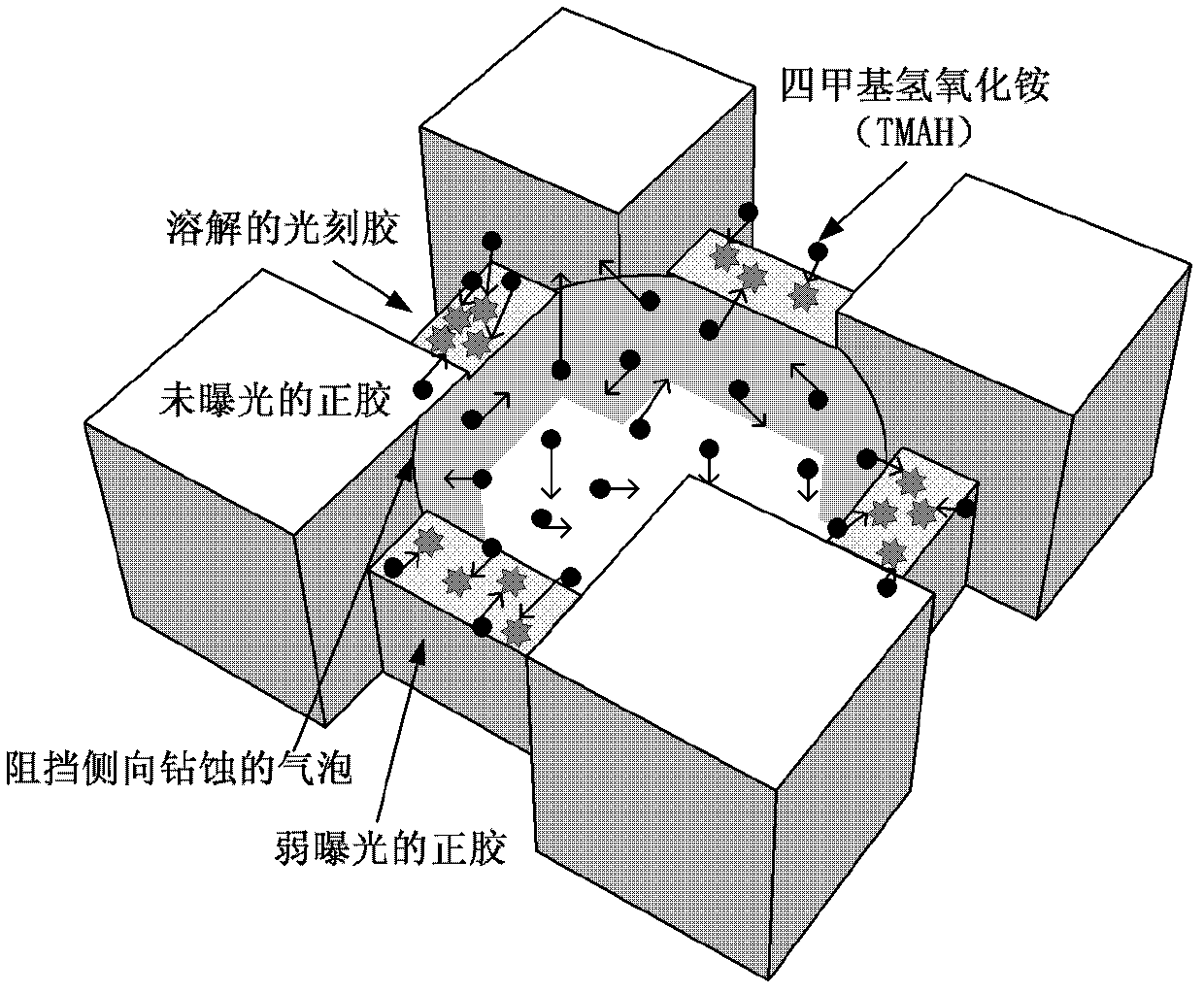
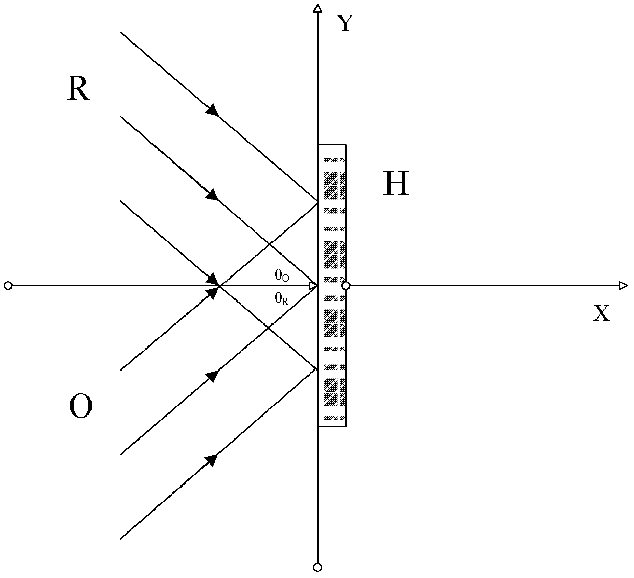
[0043] (5) Vertical cross exposure: Rotate the rotating bracket so that the angle between the light beam and the high-reflection flat mirror on the rotating ...


PUM

PropertyMeasurementUnit
thicknessaaaaaaaaaa
thicknessaaaaaaaaaa
depthaaaaaaaaaa

Abstract

The invention relates to a preparation method of a sub-micron-sized two-dimensional dielectric cylindrical photonic crystal, and the preparation method comprises: depositing Si3N4 by plasma-enhanced chemical vapor deposition (PECVD), carrying out spin coating, soft baking and vertical crossover exposure, baking after exposure, developing step by step, etching Si3N4 by reactive ion etching (RIE), removing the photoresist, etching the substrate material by inductively coupled plasma etching (ICP) and removing Si3N4. Through the preparation method, the problem that the two-dimensional dielectric cylindrical photonic crystal is difficult to prepare by using a positive photoresist in holographic interferometry is solved. Compared with electron beam exposure and other methods, the preparation method has the advantages of simplicity in operation, low price, precise control, large-area preparation and the like, meets the need of the preparation of the sub-micron-sized two-dimensional dielectric cylindrical photonic crystal and has good application prospects.

Description

technical field [0001] The invention belongs to the field of preparation of photonic crystals, in particular to a preparation method of submicron-sized two-dimensional dielectric column photonic crystals. Background technique [0002] The concept of photonic crystals was developed in 1987 by E.Yablonvitch [Inhibited spontaneous emission in solid-state physics and electronics.Phys Rev Lett, 1987,58(20):2059] of Bell Laboratories of the United States and S.John of Princeton University [ Strong localization of photons in certain disordered dielectric.Phys Rev Lett,1987,58(23):2486] respectively proposed when discussing how to suppress spontaneous emission and photon localization in disordered dielectric materials. It is composed of different dielectric materials It is composed of a periodic arrangement of constant dielectric materials. Due to the periodicity, the dispersion curve of the light wave propagating in it will form a band structure. There may be a photon band gap simi...

Claims


Application Information

Patent Timeline
Patent Type & Authority Patents(China)
IPC IPC(8): C23F1/02C30B33/10H01L21/308H01L21/467G03F7/20
Inventor 曹远迎李耀耀张永刚顾溢王凯
Owner SHANGHAI INST OF MICROSYSTEM & INFORMATION TECH CHINESE ACAD OF SCI
Why Eureka
Try Eureka