
A preparation method of nano-slit array of electron emission source of SED display

An electron emission source and electron emission technology, applied in the manufacture of discharge tubes/lamps, electrode system manufacturing, circuits, etc., can solve the problems of crack uncertainty, cracks on the surface of electron emission films, etc., and achieve accurate and controllable crack positions , to ensure the effect of uniformity

Inactive Publication Date: 2011-11-30
XI AN JIAOTONG UNIV
View PDF3 Cites 9 Cited by
  • Summary
  • Abstract
  • Description
  • Claims
  • Application Information

AI Technical Summary

Problems solved by technology

There are two problems in the process of manufacturing SED nanoslits in this technology: one is that the location of the cracks is uncertain, and the other is that SEDs usually use glass as the substrate, and the degree of strain under stress is not enough to form on the surface of the electron emission film. Cracks

Method used


Image

  • A preparation method of nano-slit array of electron emission source of SED display
  • A preparation method of nano-slit array of electron emission source of SED display
  • A preparation method of nano-slit array of electron emission source of SED display

Examples


Embodiment Construction

[0031] The present invention will be described in further detail below in conjunction with the accompanying drawings.

[0032] A preparation method of an SED display electron emission source nano-slit array, comprising the following steps:

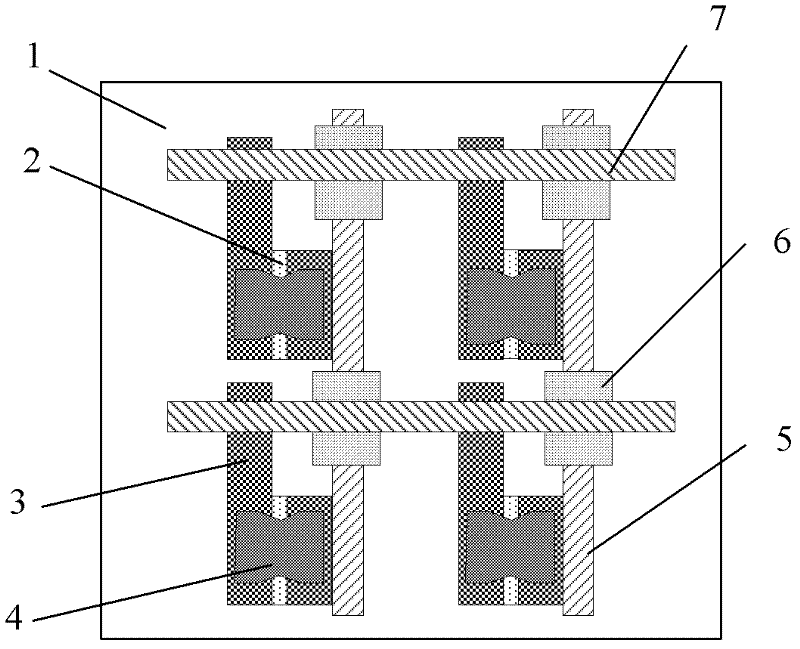
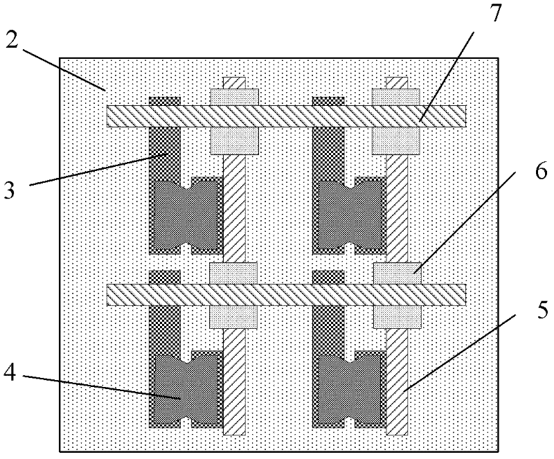
[0033] The first step is to manufacture a SED electron emission source pattern structure including a laser photoexpandable polymer material layer: a layer of laser photoexpandable polymer material is introduced between the transparent substrate and the electron emission material film with a stress concentration gap, Form a sandwich structure of "transparent substrate-laser photo-expandable polymer material-electron emission material". The laser photo-expandable polymer material adopts PMMA, PS or PI, which can have volume expansion characteristics under laser beam irradiation.

[0034] The introduction method of laser photoexpandable polymer material in the electron emission source pattern structure is divided into the overall introduction...


PUM


Abstract

The invention relates to a preparation method of an electron emission source nano seam array of a surface conduction electron emitter display (SED). A layer of a laser photoexpansion polymer material is introduced between a transparent base material and an electron emission thin film material with a stress concentration opening, so that a sandwich structure of the transparent base material, the laser photoexpansion polymer material and the electron emission material is formed; laser irradiates the laser photoexpansion polymer material in a seam of a lead electrode on one side, which does not has an electron emission source pattern structure, of the transparent base material, so that the volume of the laser photoexpansion polymer material is expanded and a pulling stress is generated inside the electron emission thin film material on the surface of the laser photoexpansion polymer material; and when the pulling stress reaches a breakage limit of the thin film material, the electron emission thin film material is broken to form a nano crack structure. In the method, by introducing the laser photoexpansion polymer material, the problem of a stress source required by breakage of the electron emission thin film can be solved and the position of a crack can be controlled precisely; meanwhile, array mirror scanning is realized by an in-situ tunnel current control method, and the uniformity of electron emission characteristics of array nano seams can be guaranteed.

Description

technical field [0001] The invention belongs to the technical field of micro-nano devices and display devices, and in particular relates to a method for preparing a nano-slit array of an electron emission source of an SED display. Background technique [0002] Flat panel display technology has a wide range of application fields and huge market prospects, and is one of the important pillars of my country's information industry. Among them, the manufacture of display panels is its core. At present, LCD (Liquid Crystal Display) and PDP (Plasma Display Panel) are the mainstream flat panel display devices in the industry, which have been commercialized on a large scale and are undergoing continuous technological upgrading; The next-generation flat panel display technology in the "post-LCD era" or "post-PDP era" has been given great attention, and a large number of basic research and technology development have been launched. Among them, organic light-emitting display OLED (Orga...

Claims


Application Information

Patent Timeline
IPC IPC(8): H01J9/02B81C1/00
Inventor 邵金友丁玉成刘红忠李祥明缪林林李欣
Owner XI AN JIAOTONG UNIV
Learn More