
Complementary Metal Oxide Semiconductor Transistor Fabrication Method

A technology of oxide semiconductors and complementary metals, applied in semiconductor/solid-state device manufacturing, electrical components, circuits, etc., can solve the problems of increased overlap capacitance, inconsistency, reduced transistor switching speed and transient characteristics, etc., to achieve overlap The effect of reducing capacitance, reducing process cost and improving production efficiency

Inactive Publication Date: 2011-11-30
CSMC TECH FAB1 +1
View PDF4 Cites 0 Cited by
  • Summary
  • Abstract
  • Description
  • Claims
  • Application Information

AI Technical Summary

Problems solved by technology

[0005] In the process of prior art CMOS transistors, the P-type heavily doped region of the PMOS transistor usually adopts boron ions as dopant ions, but the diffusion speed of the boron ions in the semiconductor substrate is faster; the diffusion speed is faster The boron ions in the semiconductor substrate will diffuse laterally and vertically, and the vertical diffusion of the boron ions will cause the junction depth of the P-type heavily doped region to change, so that the junction depth of the P-type heavily doped region is different from that of the N-type The heavily doped region is inconsistent; the lateral diffusion of the boron ions increases the overlapping capacitance between the source / drain region and the gate electrode of the PMOS transistor, and the increased overlapping capacitance will reduce the switching speed and transient characteristics of the transistor

Method used


Image

  • Complementary Metal Oxide Semiconductor Transistor Fabrication Method
  • Complementary Metal Oxide Semiconductor Transistor Fabrication Method
  • Complementary Metal Oxide Semiconductor Transistor Fabrication Method

Examples


Embodiment Construction

[0023] In the CMOS transistor manufacturing process of the prior art, the P-type heavily doped region of the PMOS transistor is formed by ion implantation, and the doping ions in the P-type heavily doped region in the PMOS transistor are usually boron ions, and the boron ions are formed on the semiconductor substrate. The diffusion speed in the bottom is fast; in the prior art, annealing treatment is required after the implantation of the heavily doped region is completed, and in the annealing treatment, the boron ions in the P-type heavily doped region will Diffusion continues above, that is, secondary diffusion occurs. The secondary diffusion of boron ions causes the doping curve of the P-type heavily doped region to deviate from the original doping curve after ion implantation. In particular, after the secondary diffusion, the P The doping curve of the N-type heavily doped region does not match the doping curve of the N-type heavily doped region, and the mismatched doping cu...


PUM

PropertyMeasurementUnit
Thicknessaaaaaaaaaa

Abstract

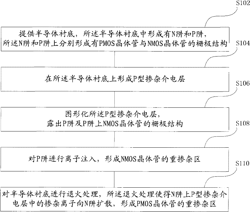
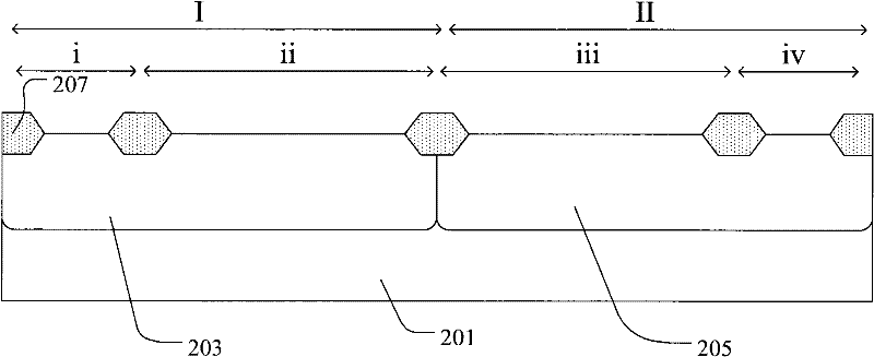
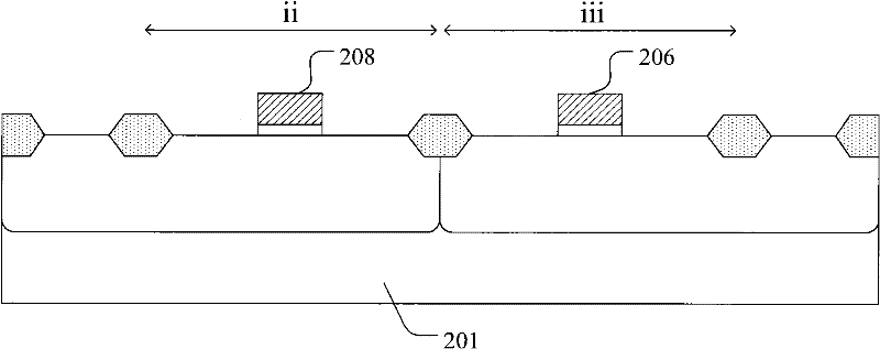
A method for manufacturing a complementary metal oxide semiconductor transistor, comprising: providing a semiconductor substrate, an N well and a P well are formed in the semiconductor substrate, and a PMOS transistor and an NMOS transistor are respectively formed on the N well and the P well. Gate structure; forming a P-type doped dielectric layer on the semiconductor substrate; patterning the P-type doped dielectric layer to expose the P well and the gate structure of the NMOS transistor on the P well; performing ion implantation on the P well , forming the heavily doped region of the NMOS transistor; the semiconductor substrate is annealed, and the annealing treatment causes the dopant ions in the P-type doped dielectric layer on the N well to diffuse to the N well, forming a heavily doped PMOS transistor Miscellaneous area. The ion doping of the P-type heavily doped region is realized by the self-doping diffusion process, which avoids the secondary diffusion effect of dopant ions in the P-type heavily doped region, making the junction depth of the heavily doped region of the PMOS transistor and the junction depth of the NMOS transistor Knot deep to match.

Description

technical field [0001] The present invention relates to the technical field of semiconductors, and more specifically, the present invention relates to a manufacturing method of a complementary metal oxide semiconductor (CMOS) transistor. Background technique [0002] With the continuous advancement of integrated circuits, that is, IC technology, the number of components integrated on the same chip has evolved from the initial tens of hundreds to the present millions. The performance and complexity of current ICs are far beyond what could have been imagined at the beginning. In order to meet the requirements of complexity and circuit density (ie: the number of devices integrated into a certain area), the minimum feature size, which is known as the "geometric line width" of the device, is getting smaller and smaller with the innovation of process technology. Today, the minimum line width of semiconductor devices is less than 65 nanometers. [0003] With the further shrinkage...

Claims


Application Information

Patent Timeline
IPC IPC(8): H01L21/8238H01L21/225
Inventor 桂林春张明敏邵永军王乐
Owner CSMC TECH FAB1
Learn More