eeprom core structure embedded in bcd process and its forming method

A nuclear structure and process technology, applied in the direction of instruments, semiconductor devices, electrical components, etc., can solve the problems of loss of industrial production, complex and complicated process flow, etc., and achieve the effect of reducing process complexity

Active Publication Date: 2011-11-30
ADVANCED SEMICON MFG CO LTD
View PDF2 Cites 9 Cited by
  • Summary
  • Abstract
  • Description
  • Claims
  • Application Information

AI Technical Summary

Problems solved by technology

The conventional BCD process is also very complicated, including low-voltage CMOS transistors, medium and high-voltage LDNMOS transistors, bipolar transistors, resistors, capacitors and other devices. The basic photolithography level of the BCD process (including two metal layers) is more than 21 layers.
Therefore, if the traditional EERPOM core structure formation process is simply embedded into the BCD process, its process flow will become too complicated and lose the meaning of industrial production

Method used


Image

  • eeprom core structure embedded in bcd process and its forming method
  • eeprom core structure embedded in bcd process and its forming method
  • eeprom core structure embedded in bcd process and its forming method

Examples


Embodiment Construction

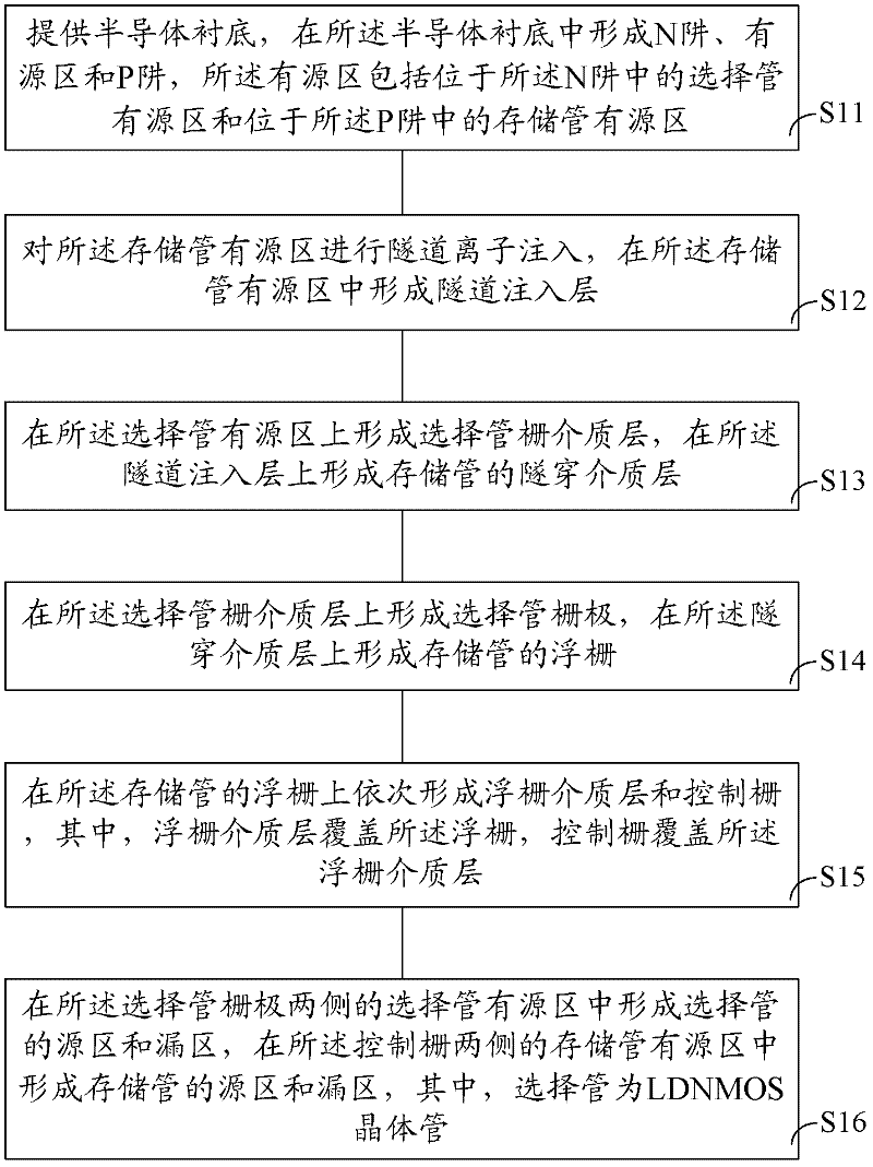
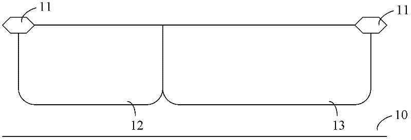
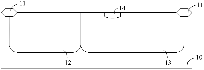
[0033] The formation process of the conventional EEPROM core structure in the prior art and the process steps of the BCD process are relatively complicated. If the EEPROM is simply embedded in the BCD process, the process steps of the two will be superimposed, which will lead to an overly complicated process, which is not conducive to large-scale of industrial production.

[0034] The selection transistor in the EEPROM core structure embedded in the BCD process of the embodiment of the present invention adopts the LDNMOS transistor, and the LDNMOS transistor can be formed by using the BCD standard process, which is beneficial to reduce its process complexity.

[0035] In addition, in the method for forming the EEPROM core structure embedded in the BCD process of the embodiment of the present invention, the process of tunnel ion implantation is added to the standard BCD process to form the tunnel implantation layer of the storage tube, which is formed by conventional steps in th...


PUM


Abstract

The invention provides an electrically erasable programmable read-only memory (EEPROM) core structure formed by a process embedded into a monolithic integration process of manufacturing a bipolar transistor, a complementary metal oxide semiconductor (CMOS) device and a double-diffusion metal oxide semiconductor (DMOS) device on an identical chip (BCD) and a forming method. The EEPROM core structure formed by the process embedded into the BCD process comprises a selectron and a memotron which are connected in series, wherein the selectron is a laterally diffused n-CHANNEL metal oxide semiconductor (LDNMOS) transistor. In the invention, the forming process of the EEPROM core structure can be embedded into the BCD process to achieve favorability for reducing the complexity of the process.

Description

technical field [0001] The invention relates to the technical field of semiconductor devices and semiconductor technology, in particular to an EEPROM core structure embedded in BCD technology and a forming method thereof. Background technique [0002] The BCD process is a monolithic integration process technology that can produce bipolar transistors (Bipolar), complementary metal oxide field effect transistors (CMOS) and double diffused metal oxide field effect transistors (DMOS) on the same chip ) device, referred to as the BCD process. Since the BCD process combines the respective advantages of the above three devices, the BCD process has received more and more attention. [0003] Products such as system-on-chip (SOC) formed by BCD technology can be applied to automotive electronics, power management, etc. In such applications, it is often necessary to integrate electrically erasable programmable read-only memory (EEPROM) in the product, but the traditional Both the BCD ...

Claims


Application Information

Patent Timeline
Patent Type & Authority Applications(China)
IPC IPC(8): H01L27/115G11C16/04H01L21/8247
CPCH01L29/788H01L27/11546H01L21/8249H01L29/7881H01L29/66825H10B41/49
Inventor 刘建华
Owner ADVANCED SEMICON MFG CO LTD
Why Eureka
Try Eureka