Manufacturing method of oriented nano-fiberized three-dimensional stereoscopic interdigital electrode of semiconductor gas-sensitive sensor

A gas-sensing sensor and interdigital electrode technology, which is applied in the production field of directional nanofiber three-dimensional interdigital electrodes, can solve problems such as large power consumption of electrodes, and achieve the effects of increasing surface area, improving sensitivity, and solving contradictions.

Active Publication Date: 2011-12-07
XI AN JIAOTONG UNIV
View PDF8 Cites 13 Cited by
  • Summary
  • Abstract
  • Description
  • Claims
  • Application Information

AI Technical Summary

Problems solved by technology

[0006] (2) The operating temperature of the semiconductor gas sensor is relatively high. To ensure that it works in a stable state, it must be heated, while the traditional flat interdigitated electrode consumes a lot of power

Method used


Image

  • Manufacturing method of oriented nano-fiberized three-dimensional stereoscopic interdigital electrode of semiconductor gas-sensitive sensor
  • Manufacturing method of oriented nano-fiberized three-dimensional stereoscopic interdigital electrode of semiconductor gas-sensitive sensor
  • Manufacturing method of oriented nano-fiberized three-dimensional stereoscopic interdigital electrode of semiconductor gas-sensitive sensor

Examples


Embodiment Construction

[0022] The preparation method of this law invention comprises the following steps:

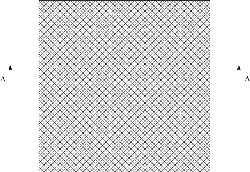
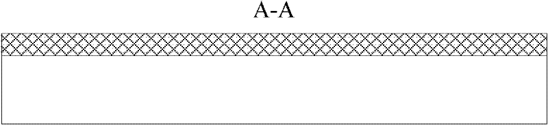
[0023] In the first step, referring to Figure 1(a), (b), apply a layer of ultraviolet photoresist with a thickness of 200nm on the single crystal silicon substrate by using the glue-spinning process;

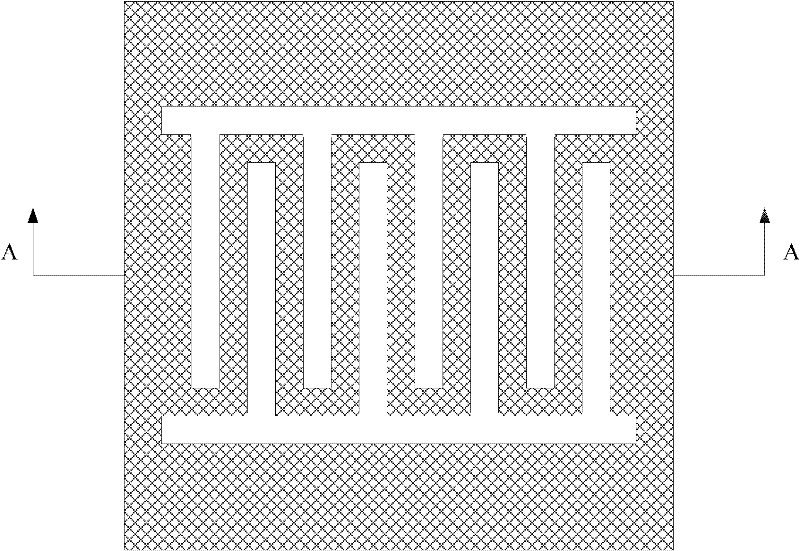
[0024] In the second step, referring to Fig. 6 (a), (b), make an interdigital electrode mask according to the parameters of the interdigital electrode to be prepared, wherein the interdigital length is 10mm, the interdigital width is 1mm, and the interdigital spacing is 1mm. There are 4 pairs of interdigitated pairs; then use the interdigitated electrode mask as a cover to use ultraviolet (UV) photolithography to obtain photoresist interdigitated electrodes as shown in Figure 2 (a), (b).

[0025] In the third step, the photoresist layer obtained in the previous step is used as a cover, using C 4 f 8 : 180sccm (milliliters per minute), time: 10s; SF 6 : 100sccm (milliliters per minute), time: ...


PUM


Abstract

The invention relates to semiconductor gas-sensitive sensor technology, and discloses a manufacturing method of an oriented nano-fiberized three-dimensional stereoscopic interdigital electrode of a semiconductor gas-sensitive sensor. The method comprises the following steps: firstly transferring a pattern of an interdigital electrode to a photoresist layer by a traditional photoetching process, etching a monocrystalline silicon substrate by a dry method with the photoresist layer as a mask so as to prepare oriented nano-fibers, sputtering a layer of Pt as a conducting layer on the fiber surfaces by a magnetron sputtering process, and finally peeling off the photoresist layer by a chemical method to obtain the oriented nano-fiberized three-dimensional stereoscopic interdigital electrode of a semiconductor gas-sensitive sensor. Compared with traditional plate interdigital electrodes, the oriented nano-fiberized three-dimensional stereoscopic interdigital electrode contains silicon nanofibers with high specific surface areas which can effectively increase the surface area of the electrode without decreasing interdigital pair numbers, thus can effectively increase the sensitivity of the sensitive electrode, and solves the contradictory relation between the interdigital pair numbers of traditional plate interdigital electrodes and surface areas.

Description

technical field [0001] The invention belongs to semiconductor gas sensor technology, in particular to a manufacturing method of directional nanofiberized three-dimensional interdigitated electrodes of a semiconductor gas sensor. Background technique [0002] Compared with other gas sensor technologies, semiconductor gas sensor technology has unparalleled advantages, and has been widely researched and applied. Such as small size, high sensitivity, long service life, low cost, simple measurement circuit, easy to use, easy to integrate and multi-functional, easy to interface with microcomputer, etc., and are widely used in coal, chemical, petroleum industry, traffic monitoring , environmental protection, meteorological monitoring, medical care, automatic control and household alarms and other fields, to detect toxic and harmful gases, flammable and explosive gases, industrial waste gases and environmental pollution gases. [0003] The two key technologies in semiconductor gas ...

Claims


Application Information

Patent Timeline
Patent Type & Authority Applications(China)
IPC IPC(8): G01N27/00
Inventor 刘红忠丁玉成陈邦道郑杰卢秉恒
Owner XI AN JIAOTONG UNIV
Why Eureka
Try Eureka