A method for increasing back gate threshold voltage of soi-pmos device

A threshold voltage, back-gate technology, applied in semiconductor devices, semiconductor/solid-state device manufacturing, circuits, etc., can solve the problems of increasing process complexity, device damage, and increasing costs, and achieve back-gate threshold voltage and improve threshold voltage. Effect

Inactive Publication Date: 2011-12-07
INST OF MICROELECTRONICS CHINESE ACAD OF SCI
View PDF2 Cites 4 Cited by
  • Summary
  • Abstract
  • Description
  • Claims
  • Application Information

AI Technical Summary

Problems solved by technology

To increase the threshold voltage of the back gate by doping the back gate channel, first of all, the range of the threshold voltage increase cannot be precisely controlled, because the doping concentration cannot be precisely controlled; in addition, this will increase the complexity of the process, increase the cost of manufacturing, and doping Miscellaneous processes (such as ion implantation) can cause damage to the device and produce other effects

Method used


Image

  • A method for increasing back gate threshold voltage of soi-pmos device
  • A method for increasing back gate threshold voltage of soi-pmos device
  • A method for increasing back gate threshold voltage of soi-pmos device

Examples


Embodiment Construction

[0018] The technical solution of the present invention will be described in detail below in conjunction with the accompanying drawings and embodiments.

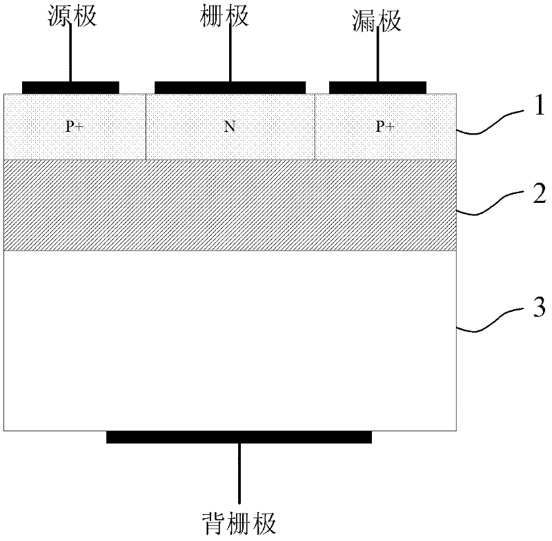
[0019] Such as figure 1 as shown, figure 1 It is an SOI-PMOS device that can be used in the present invention. The SOI silicon wafer comprises a top silicon film (1), an insulating oxide layer (2) and a silicon substrate (3), and an SOI-PMOS device is prepared on the top silicon film (1). The SOI material is a commercial conventional oxygen ion implantation isolation (SIMOX) sheet, and other thermal bonding and smart-cut (Smart-Cut) sheets can also be used. For a normal working SOI-PMOS device, the gate and drain are connected to the power supply potential (Vdd), and the source and back gate are connected to the ground potential (Vss).

[0020] Bulk silicon PMOS devices in the prior art generally have only three terminals, namely: gate, source and drain, and only focus on the threshold voltage of the gate. The general met...


PUM


Abstract

The invention relates to the technical field of SOICMOS semiconductor integrated circuits, in particular to a method for increasing the back gate threshold voltage of an SOI-PMOS device. The method specifically includes the following steps: connect the source, drain, and gate of the SOI-PMOS device to the ground potential, connect the back gate of the SOI-PMOS device to a negative DC voltage with an absolute value greater than 80V, and continue for more than 10 seconds time. The invention tests the back gate threshold voltage of the SOI-PMOS device, improves the threshold voltage of the back gate channel opening of the SOI-PMOS device, and can realize the increase of the back gate threshold voltage of the SOI-PMOS device and the reduction of the off-state leakage current .

Description

technical field [0001] The invention relates to the technical field of SOI CMOS semiconductor integrated circuits, in particular to a method for increasing the back gate threshold voltage of an SOI-PMOS device. Background technique [0002] SOI (Silicon-On-Insulator) technology refers to the fabrication of devices and circuits on a silicon film on an insulating layer (BOX), which is different from the ordinary bulk silicon technology that directly manufactures devices and circuits on a semiconductor substrate. Complete dielectric isolation is achieved between devices, so SOI-CMOS integrated circuits essentially avoid the latch-up effect of bulk silicon CMOS circuits; in addition, SOI devices have small short-channel effects, can naturally form shallow junctions, and leak current Small, with excellent subthreshold characteristics. SOI-CMOS integrated circuits with no latch, high speed, low power supply voltage, low power consumption, radiation resistance and high temperature...

Claims


Application Information

Patent Timeline
IPC IPC(8): H01L21/336H01L21/28
Inventor 梅博毕津顺韩郑生
Owner INST OF MICROELECTRONICS CHINESE ACAD OF SCI
Why Eureka
Try Eureka