Supercharge Your Innovation With Domain-Expert AI Agents!

Electrostatic-proof protection circuit

A protection circuit, anti-static technology, applied in emergency protection circuit devices, emergency protection circuit devices for limiting overcurrent/overvoltage, circuit devices, etc., can solve problems such as distortion

Active Publication Date: 2014-04-09
SHANGHAI MOUNTAIN VIEW SILICON
View PDF6 Cites 1 Cited by
  • Summary
  • Abstract
  • Description
  • Claims
  • Application Information

AI Technical Summary

Problems solved by technology

However, because the substrate of the PMOS transistor 33 is connected to the power supply terminal 32, when the signal input by the signal source 30 is higher than the power supply voltage of the power supply terminal 32, the PMOS transistor 33 will be turned on, and the signal input by the signal source 30 will be clamped at the power supply. Deformation occurs on the voltage potential, resulting in distortion

Method used


Image

  • Electrostatic-proof protection circuit
  • Electrostatic-proof protection circuit
  • Electrostatic-proof protection circuit

Examples


no. 1 example

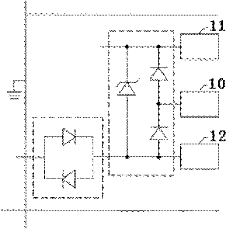
[0048] see Figure 4A to Figure 4C , which is a circuit diagram showing the first embodiment of the antistatic protection circuit of the present invention. As shown in the figure, the anti-static protection circuit of the present invention includes a first diode D1, a second diode D2, a first PMOS transistor M1, and a first PMOS transistor M2. components are described in detail.

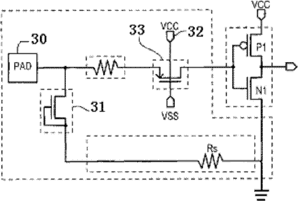
[0049] The anode of the first diode D1 is connected to the ground terminal VSS, its cathode is connected to the cathode of the second diode D2, and a first tap point a is formed at the connection, and the anode of the second diode D2 is connected to the signal Source VIN.

[0050] The first PMOS transistor M1 has a source s1, a gate g1, a drain d1 and a substrate, the substrate is connected to the source s1 and then connected to the first tap point a, and the gate g1 is connected to the first tap point a through a capacitor C1. The signal source VIN is connected, and its gate g1 is also connected ...

no. 2 example

[0059] see figure 2 , is to show the circuit diagram of the second embodiment of the antistatic protection circuit of the present invention, wherein, with the antistatic protection circuit of the foregoing embodiment (such as Figures 4A to 4C Shown) the same or similar components are represented by the same or similar symbols, and detailed descriptions are omitted to make the description of this case clearer and easier to understand.

[0060] The biggest difference between the anti-static protection circuit of the second embodiment and the anti-static protection circuit of the first embodiment is that the anti-static protection circuit of the first embodiment uses the ground terminal VSS as the static discharge point of the signal source VIN; The anti-static protection circuit of the second embodiment uses the power supply terminal VDD' as the electrostatic discharge point of the signal source VIN'. In addition, because the static discharge point is selected differently, in ...

no. 3 example

[0068] see Figure 6 , is to show the circuit diagram of the third embodiment of the antistatic protection circuit of the present invention, wherein, with the antistatic protection circuit of the foregoing embodiment (such as Figures 4A-4C as well as Figures 5A-5C Shown) the same or similar components are represented by the same or similar symbols, and detailed descriptions are omitted to make the description of this case clearer and easier to understand.


PUM


Abstract

The invention relates to an electrostatic-proof protection circuit which comprises a first diode, a second diode, a first PMOS (positive-channel metal oxide semiconductor) tube and a second PMOS tube, wherein an anode of the first diode is connected with a first input source, the anode of the second diode is connected with a second input source, cathodes of the first and the second diodes are connected, a first tapping point is formed at the junction, connected with a source (s1) which is arranged in the first PMOS tube and connected with a substrate of the first PMOS tube and simultaneously connected with the source (s2) which is arranged in the second PMOS tube and connected with the substrate of the second PMOS tube, a drain (d1) of the first PMOS tube is connected with the second input source, a gate (g1) of the first PMOS tube is connected with the second input source through a capacitor, the gate (g1) of the first PMOS tube is further connected with the first input source through a resistor, the gate (g2) of the second PMOS tube is connected with the second input source through the resistor, the gate (g2) of the second PMOS tube is further connected with the first input source through the capacitor and the drain (d2) of the second PMOS tube is connected with the first input source, wherein the first or the second input source is a signal source. Therefore, the problem that input signals are clamped because the swing amplitude of the input signals exceeds the voltage of a power supply or is lower than the ground can be solved.

Description

technical field [0001] The invention relates to a semiconductor technology, in particular to an antistatic protection circuit. Background technique [0002] Designing an antistatic (Electrostatic Discharge; ESD) protection circuit on an input / output circuit of a chip is a necessary work for chip design and manufacture. For example, US Patent Publication No. US6456472B1, US Patent Publication No. US6751077B2, and US Patent Publication No. US7855862B1 have proposed ESD discharge protection with different circuit structures. [0003] see figure 1 , that is, a schematic diagram showing the circuit structure of a general multi-power domain ESD discharge protection method disclosed in the US Patent No. US6456472B1 invention patent. Add a diode between the terminal 11, and add a reverse diode between the signal source 10 and the ground terminal 12, so that when the signal source 10 has a high or low charge input, it can be discharged to the power supply terminal 11 or the ground ...

Claims


Application Information

Patent Timeline
Patent Type & Authority Patents(China)
IPC IPC(8): H02H9/04
Inventor 许刚
Owner SHANGHAI MOUNTAIN VIEW SILICON
Features
  • R&D
  • Intellectual Property
  • Life Sciences
  • Materials
  • Tech Scout
  • Unparalleled Data Quality
  • Higher Quality Content
  • 60% Fewer Hallucinations
Learn More