High-temperature solar selective absorbing coating with SiO2 and Cr2O3 double-ceramic structure and preparation method thereof
A technology for absorbing coating and solar energy, applied in the field of solar energy utilization, can solve the problems of unstable microstructure and physical properties, low deposition rate, long production cycle, etc., and achieve stable microstructure and physical properties, simple preparation process, and easy operation. handy effect
- Summary
- Abstract
- Description
- Claims
- Application Information
AI Technical Summary
Problems solved by technology
Method used
Image
Examples
preparation example Construction
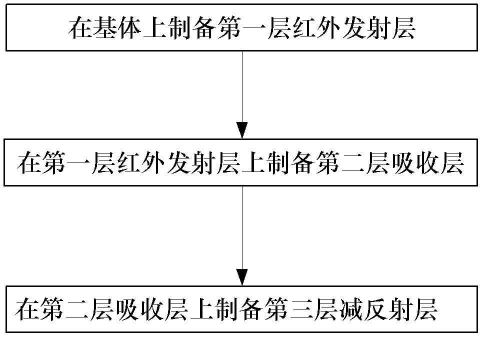
[0026] The invention provides a kind of SiO 2 and Cr 2 o 3 The preparation method of the double ceramic structure high temperature solar energy selective absorption coating, such as figure 2 shown, including the following steps:
[0027] Step 1: preparing the first infrared emitting layer on the substrate;
[0028] A pure metal target DC or intermediate frequency magnetron sputtering method is adopted. The pure metal target is Cu target or Ag target (purity 99.99%), prepared with Ar gas as the sputtering gas, and the substrate is made of high-speed steel. Before sputtering, the vacuum chamber was pre-evacuated to a background vacuum of 4×10 -3 ~5×10 -3 Pa, the inert gas Ar gas is introduced as the sputtering atmosphere, the Ar gas flow rate is 100-140sccm, the sputtering distance is adjusted to 130-150mm, and the sputtering pressure is adjusted to 3×10 -1 ~4×10 -1 Pa. Turn on the power supply of the sputtering target of the pure metal target, adjust the sputtering vol...
Embodiment 1
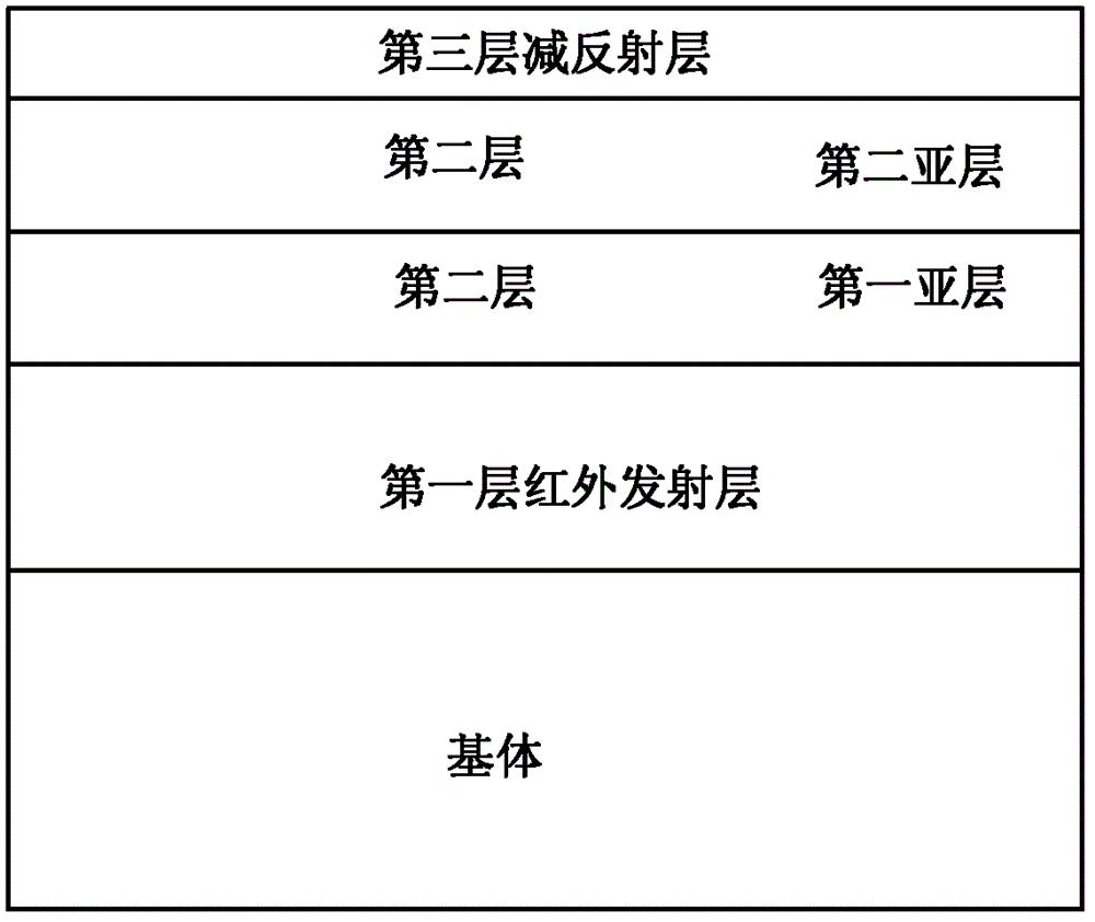
[0035] This embodiment provides a kind of solar energy selective absorption coating, comprises three coatings namely the first layer infrared reflection layer, the second layer absorption layer, the third layer anti-reflection layer, the thickness of the first layer is 200nm, the second layer is total The thickness is 150nm, the thickness of the first sublayer is 90nm, the thickness of the second sublayer is 60nm, and the SiO in the first sublayer 2 The volume percentage is 60%, the second sublayer SiO 2 The volume percentage is 40%, and the thickness of the third layer is 60nm. The preparation steps are as follows:
[0036] Step 1: preparing the first infrared emitting layer on the substrate;
[0037] The Cu target with a purity of 99.99% is selected, and the base material is high-speed steel. Before sputtering, the vacuum chamber was pre-evacuated to a background vacuum of 4.5×10 -3 Pa, the inert gas Ar is introduced as the sputtering atmosphere, the Ar gas flow rate is ...
Embodiment 2
[0045] The present embodiment provides a kind of SiO 2 and Cr 2 o 3 The dual-ceramic structure high-temperature solar selective absorption coating, which includes three layers of film, from the bottom to the surface is an infrared reflection layer, an absorption layer and an anti-reflection layer;
[0046] The first infrared reflective layer is a Cu or Ag film, located on the surface of the substrate, with a thickness of 50nm; the second absorbing layer includes two sublayer structures, both of which are SiO 2 +Cr 2 o 3 film, the thickness of the first sublayer and the second sublayer are both 50nm, and the SiO in the first sublayer 2 The volume percentage is 50%, the second sublayer SiO 2 The volume percentage is 30%, wherein the first sublayer is adjacent to the first infrared reflection layer, the second sublayer is adjacent to the third antireflection layer; the third antireflection layer is SiO 2 film with a thickness of 40 nm.
[0047] The present embodiment provi...
PUM
| Property | Measurement | Unit |
|---|---|---|
| thickness | aaaaa | aaaaa |
| thickness | aaaaa | aaaaa |
| thickness | aaaaa | aaaaa |
Abstract
Description
Claims
Application Information

