Cr series high-temperature solar selective absorbing coating and preparation method thereof
A technology for absorbing coatings and solar energy, applied in the field of solar energy utilization, can solve the problems of low process deposition rate, long production cycle, complex process, etc., and achieve the effects of low price, low emissivity, and simple preparation process
- Summary
- Abstract
- Description
- Claims
- Application Information
AI Technical Summary
Problems solved by technology
Method used
Image
Examples
preparation example Construction
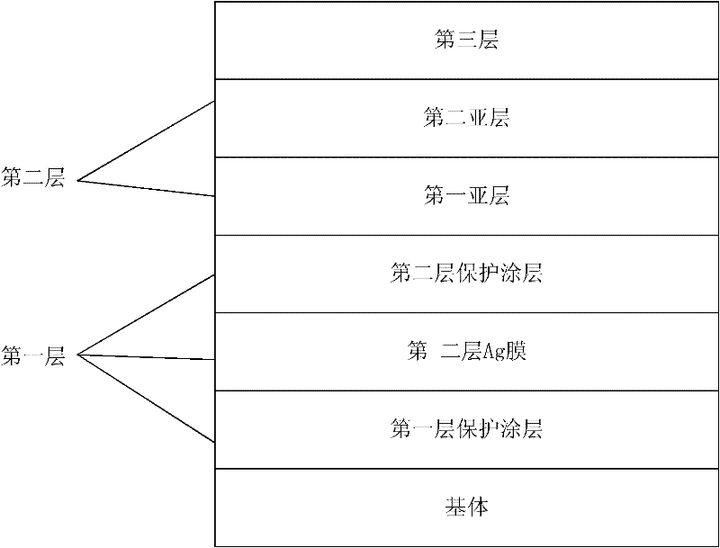
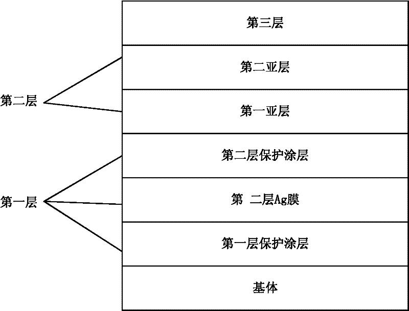
[0025] A method for preparing a Cr-based high-temperature solar selective absorption coating, comprising the following steps:
[0026] Step 1: preparing the first infrared emitting layer on the substrate;
[0027] Using pure metal target intermediate frequency magnetron sputtering method, the substrate is made of stainless steel, firstly prepare the first protective coating of the first infrared emission layer on the substrate, the pure metal target is Cr target or Al target, and Ar and O 2 The mixed gas is prepared as sputtering gas. Before sputtering, the vacuum chamber was pre-evacuated to a background vacuum of 4×10 -3 ~5×10 -3 Pa, into the inert gas Ar as the sputtering atmosphere, adjust the sputtering distance to 130 ~ 150mm, adjust the sputtering pressure to 3 × 10 -1 ~4×10 -1 Pa. Turn on the power supply of the sputtering target of the pure metal target, adjust the sputtering voltage to 380-450V, and the sputtering current to 8-10A, and prepare the first layer of...
Embodiment
[0038] Prepare a Cr-based high-temperature solar energy selective absorption coating, including three coatings, namely the first infrared reflection layer, the second absorption layer, and the third anti-reflection layer. The thickness of the first layer is 100-250nm, and the second layer is The total thickness of the layers is 110-150 nm, wherein the thickness of the first sub-layer is 60-80 nm, the thickness of the second sub-layer is 50-70 nm, and the thickness of the third layer is 30-50 nm. The preparation steps are as follows:
[0039] Step 1: preparing the first infrared emitting layer on the substrate;
[0040] An Al target with a purity of 99.99% and an Ag target with a purity of 99.99% are selected, and stainless steel is used as the base material. First prepare the first protective coating of the first infrared emission layer on the substrate, and pre-evacuate the vacuum chamber to 4.5×10 before sputtering. -3 ~5×10 -3 Pa, through the inert gas Ar and O 2 The mi...
PUM
| Property | Measurement | Unit |
|---|---|---|
| thickness | aaaaa | aaaaa |
| thickness | aaaaa | aaaaa |
| thickness | aaaaa | aaaaa |
Abstract
Description
Claims
Application Information

