Photoelectric response characteristic calibration method for two-dimensional imaging device

A technology of two-dimensional imaging and calibration method, which is used in the testing of machine/structural components, instruments, optical instruments, etc., and can solve the problems of low utilization rate of light energy, inability to achieve large-scale calibration, and unusable calibration light sources.

Active Publication Date: 2013-05-29
INST OF OPTICS & ELECTRONICS - CHINESE ACAD OF SCI
View PDF3 Cites 0 Cited by
  • Summary
  • Abstract
  • Description
  • Claims
  • Application Information

AI Technical Summary

Problems solved by technology

The advantage of the CCD calibration method based on pinhole diffraction and double-slit diffraction is that the calibration work only needs a single exposure, and there are more CCD sampling data points available, but the disadvantage is that in order to obtain more sampling data on the CCD photosensitive surface point, the size of the small hole or double slit is required to be relatively small, which leads to the low utilization rate of light energy of the above two methods, and cannot achieve a wide range of calibration, especially when the calibration light source is weak.
All of the above methods require multiple exposures, and the measurement results are greatly affected by the measurement accuracy of energy measurement and other auxiliary quantities.

Method used


Image

  • Photoelectric response characteristic calibration method for two-dimensional imaging device
  • Photoelectric response characteristic calibration method for two-dimensional imaging device
  • Photoelectric response characteristic calibration method for two-dimensional imaging device

Examples


specific Embodiment

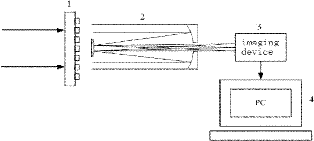
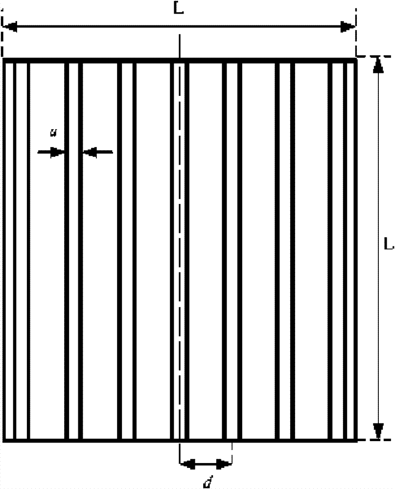
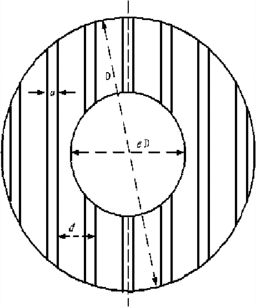
[0044] Specific embodiment: To calibrate the photoelectric response characteristics of an infrared CCD camera with unknown characteristics to a certain infrared laser. The incident beam is a parallel plane beam with a diameter of φ=120mm. The focusing optical system 2 adopts a reflective Cassegrain system. The outer diameter of the incident end is D=120mm, the central blocking ratio is ε=0.42, the effective focal length is f=2.47m, and the CCD photosensitive surface The number of pixels is 128×128, the size of a single pixel is 30μm×30μm, and the digital signal output is 14bit. According to the basic situation and experience of the infrared CCD camera, the linear response area of ​​the CCD to be measured wavelength light contains at least the gray value The range is 1000-4000 ADU, and the scribed direction of the line diffraction grating is placed in front of the vertical direction in close contact with the focusing optical system. From the above parameters, it is required tha...


PUM


Abstract

The invention relates to a photoelectric response characteristic calibration method for a two-dimensional imaging device, which comprises a ray diffraction grating, a focusing optical system, a two-dimensional imaging device to be calibrated and a computer system, wherein an incident light beam for calibrating the two-dimensional imaging device is a light beam parallel to the plane, the light beam is imaged on the photosensitive surface of the two-dimensional imaging device after being modulated by the space intensity of the ray diffraction grating and being converged by the focusing optical system, the incident light beam forms a series of diffraction sub light spots with modulated light intensity on the photosensitive surface of the two-dimensional imaging device through the beam splitting characteristic of the ray diffraction grating, a plurality of groups of measured data are fused through peak value measuring data of each diffraction sub light spot and peak value theoretical dataobtained by theoretical calculation, the measured data and the corresponding theoretical data are obtained, the two groups of data are combined for completing the photoelectric response characteristic calibration of the two-dimensional imaging device. The photoelectric response characteristic calibration method has high light energy utilization rate, is applicable to the photoelectric response characteristic calibration of the two-dimensional imaging device under the condition with strong light sources and is also applicable to weak light sources, and the calibration range is enlarged throughthe fusion of a plurality of groups of measured data.

Description

technical field [0001] The invention relates to the calibration of the photoelectric response characteristic of a two-dimensional imaging device, in particular to a calibration method of the photoelectric response characteristic of a two-dimensional imaging device based on the beam splitting characteristic of a grating. Background technique [0002] High-resolution two-dimensional imaging devices, such as CCD devices, have many advantages such as good photoelectric conversion characteristics, high sensitivity, large dynamic range and small size, and have become the core device for measuring laser beam parameters in the field of lasers. Due to the limited linear response range (dynamic range) of the imaging device, it is usually necessary to calibrate the photoelectric response characteristics of the laser beam at the wavelength of the device before measuring the parameters of the laser beam, so that the laser intensity can be properly attenuated and measured during the measur...

Claims


Application Information

Patent Timeline
Patent Type & Authority Patents(China)
IPC IPC(8): G01M11/00
Inventor 贺元兴李新阳
Owner INST OF OPTICS & ELECTRONICS - CHINESE ACAD OF SCI
Why Eureka
Try Eureka