A p-i-n type single-junction ingan solar cell

A p-i-n, solar cell technology, applied in the direction of circuits, photovoltaic power generation, electrical components, etc., can solve the problems of photoelectric conversion efficiency to be improved, less carrier collection, affecting service life, etc., to improve photoelectric conversion efficiency and improve radiation resistance capacity, prolonging the service life

Active Publication Date: 2016-03-09
CHINA ELECTRONIC TECH GRP CORP NO 18 RES INST
View PDF7 Cites 0 Cited by
  • Summary
  • Abstract
  • Description
  • Claims
  • Application Information

AI Technical Summary

Problems solved by technology

The photoelectric conversion efficiency of the above-mentioned invention patents has been improved, but quantum wells or quantum dots lead to complex processes in the epitaxial growth of the battery structure, which increases the difficulty of making the battery; the patent number is 200710062978.0, and the name is: single-junction InGaN solar cell Invention patent for the structure and manufacturing method, the structure includes: a substrate, on which is a low-temperature gallium nitride nucleation layer, a non-intentionally doped gallium nitride buffer layer, and an n-type doped In x Ga 1-x N layer, a p-type doped In x Ga 1-x N layer, the invention patent has no quantum dot or quantum well structure, the production process is simple, and the radiation resistance is strong, but the photoelectric conversion efficiency needs to be improved
[0005] The above technologies all describe the growth process of InGaN materials, which cannot be directly applied as a complete solar cell, and the collection of carriers is small, which affects the service life

Method used


Image

  • A p-i-n type single-junction ingan solar cell
  • A p-i-n type single-junction ingan solar cell
  • A p-i-n type single-junction ingan solar cell

Examples


Embodiment Construction

[0020] In order to further understand the technical content, characteristics and effects of the present invention, the following examples are given, and detailed descriptions are as follows in conjunction with the accompanying drawings:

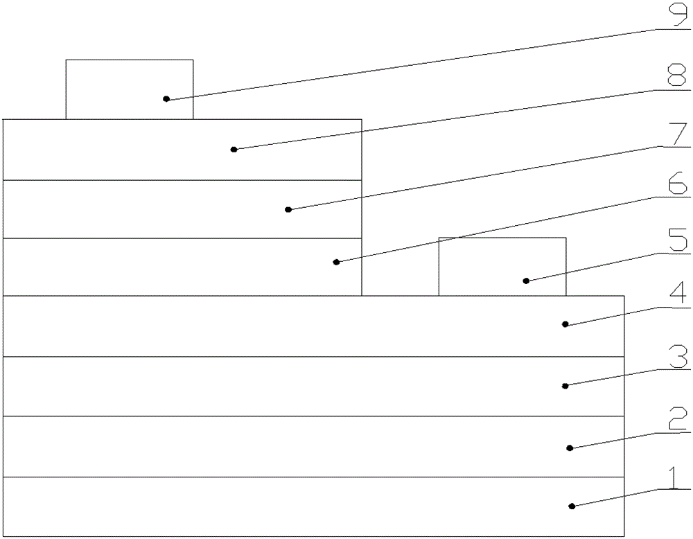
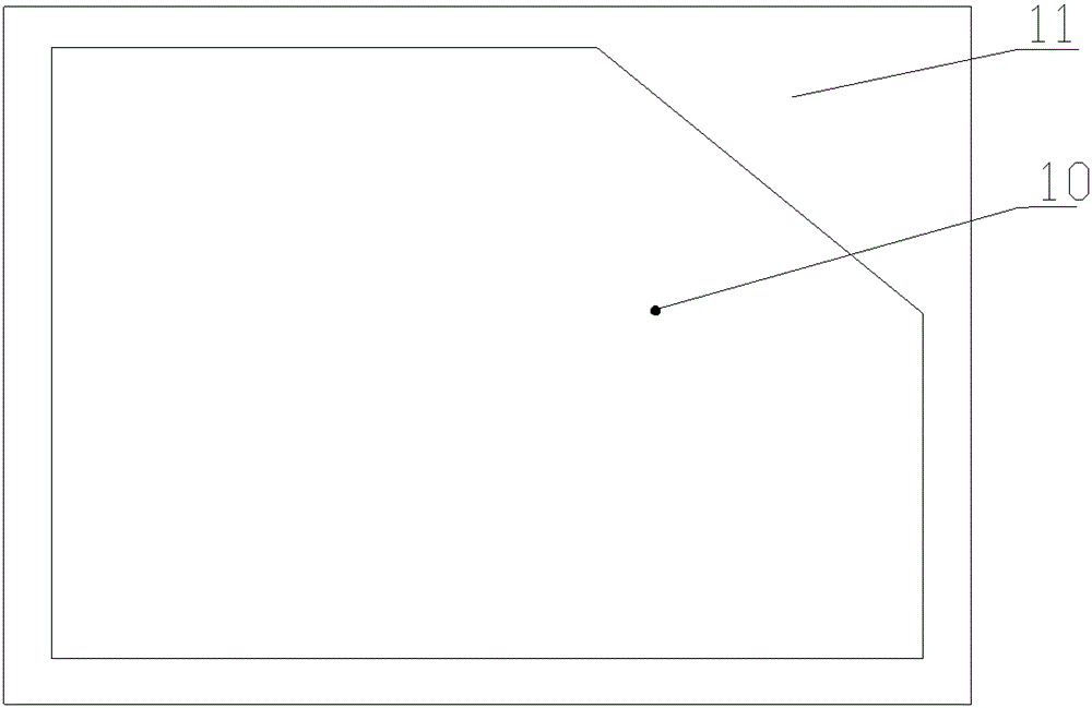
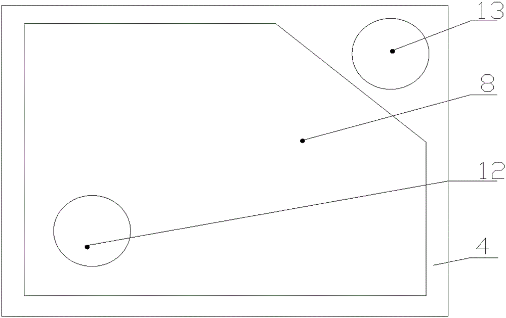
[0021] See attached Figure 1-Figure 3 .

[0022] Firstly, GaN nucleation layer 2, GaN buffer layer 3, n-GaN layer 4, i-In x Ga 1-x The specific manufacturing process of the N layer 6 and the p-GaN layer 7 is as follows:

[0023] GaN nucleation layer, the growth temperature is 500-650°C, and the thickness range is 10-35nm. This layer can increase the nucleation density on the substrate surface;

[0024] GaN buffer layer, the growth temperature is 950-1100℃, and the thickness range is 1-2.5μm. This layer can reduce the defect density of the epitaxial layer, thereby improving the crystal quality;

[0025] Si-doped n-GaN layer, the growth temperature is 600-1100°C, and the doping concentration is 1×10 18 -1×10 19 cm -3 , the thickness ran...


PUM


Abstract

The invention relates to a p-i-n type single-junction InGaN solar cell, comprising a substrate, on which there are sequentially a GaN nucleation layer, a GaN buffer layer, a Si-doped n-GaN layer and a Mg-doped p-GaN layer. The characteristics are: an i-InxGa1-xN layer is grown on the Si-doped n-GaN layer, a translucent current spreading layer is evaporated on the Mg-doped p-GaN layer, and a positive electrode is evaporated, and the Si-doped A negative electrode is vapor-deposited on the n-GaN layer. The invention adopts a mature growth process to grow an undoped i-InxGa1-xN layer on a Si-doped n-GaN layer, which improves the photoelectric conversion efficiency and is easy to prepare compared with quantum dot or quantum well structures; Plating a translucent current spreading layer and positive and negative electrodes realizes the direct application of a complete solar cell, further improves the radiation resistance and prolongs the service life of the battery.

Description

technical field [0001] The invention belongs to the technical field of solar cell structure, in particular to a p-i-n type single-junction InGaN solar cell. Background technique [0002] With the global energy crisis and the deterioration of ecological environment problems, people pay more and more attention to solar energy, an inexhaustible green energy. For a long time, people have been tirelessly looking for materials with high conversion efficiency. In recent years, the third-generation semiconductor materials GaN, InGaN, and AlGaN-represented Group III nitrides have become research hotspots. They are mainly used in optoelectronic devices and high-temperature, high-frequency, and high-power devices. The research results in 2002 showed that the forbidden band width of InN was not 1.89eV as previously reported but 0.7eV, which means that by adjusting the In composition in InGaN material, its forbidden band width can be changed from 3.4eV of GaN to that of InN. 0.7eV is co...

Claims


Application Information

Patent Timeline
Patent Type & Authority Patents(China)
IPC IPC(8): H01L31/075H01L31/0352
CPCY02E10/548
Inventor 刘如彬孙强张启明王帅康培高鹏穆杰
Owner CHINA ELECTRONIC TECH GRP CORP NO 18 RES INST
Why Eureka
Try Eureka