Fabrication method of trench type super junction device and obtained device

一种制作方法、超级结的技术,应用在半导体/固态器件制造、半导体器件、电气元件等方向,能够解决难度大、成本增加等问题,达到增加击穿电压、减低成本、工艺难度减低的效果

Inactive Publication Date: 2011-12-28
SHANGHAI HUAHONG GRACE SEMICON MFG CORP
View PDF4 Cites 14 Cited by
  • Summary
  • Abstract
  • Description
  • Claims
  • Application Information

AI Technical Summary

Problems solved by technology

Afterwards, silicon is filled in the groove to form an N / P alternate arrangement structure after CMP; however, the etching and silicon filling of deep trenches are not only difficult to realize in terms of technology, but also have the problem of increased relative cost.

Method used


Image

  • Fabrication method of trench type super junction device and obtained device
  • Fabrication method of trench type super junction device and obtained device
  • Fabrication method of trench type super junction device and obtained device

Examples


Embodiment Construction

[0017] The first embodiment of the method of the present invention comprises the following steps:

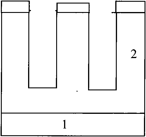
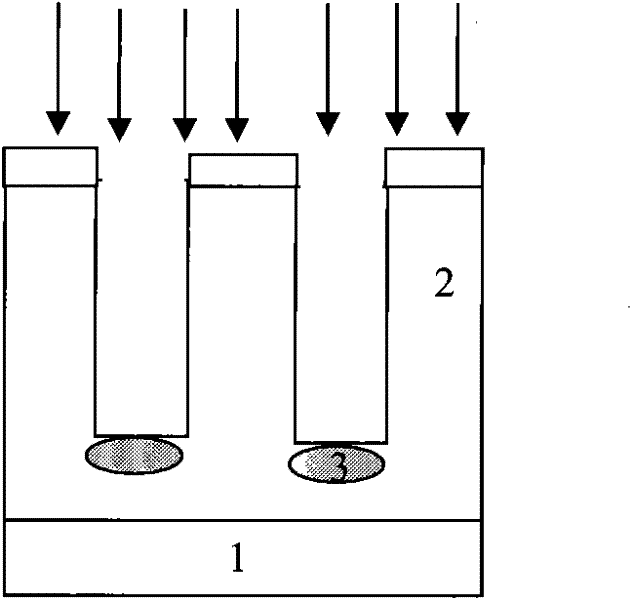
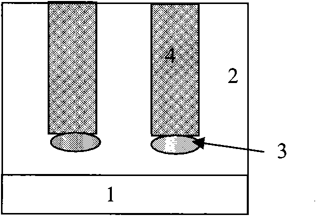
[0018] Step 1, see Figure 1A As shown, the N- epitaxial layer 2 is formed on the N+ silicon substrate 1, and the resistivity of N+ is generally 0.001-0.003 ohm.cm; the thickness and resistivity of the epitaxial layer are determined according to the requirements of device design, such as for BVDS600V device, its resistivity is generally selected at 2-10 ohm / cm, and its thickness is selected at 40-55 microns; a layer of silicon oxide film 31 is grown on the N-epitaxial layer 2 (this silicon oxide film can be used as a groove engraved etch mask, which can be used as a barrier layer during chemical mechanical polishing), and the groove pattern is obtained by groove photolithography (here, the groove can pass through the N epitaxy to the N+ substrate, or it can stay in the N epitaxy, .Depending on the requirements of the device design);

[0019] The silicon oxide film 31 can be obt...


PUM


Abstract

A method for manufacturing trench type super junction device is disclosed. The method includes the step of forming one or more P type implantation regions in the N type epitaxial layer below the bottom of each trench. By using this method, a super junction device having alternating P type and N type regions is produced, wherein the P type region is formed by P type silicon filled in the trench and P type implantation regions below the trench. The present invention can greatly improve the breakdown voltage of a super junction MOSFET.

Description

technical field [0001] The invention relates to a semiconductor device and a manufacturing method thereof. Background technique [0002] The device of super junction structure replaces the N drift region in the traditional VDMOS by using the structure of N / P alternate arrangement. It combines the well-known VDMOS process in the industry to produce a MOSFET with super junction structure. In the same situation as the traditional VDMOS, the on-resistance of the device is greatly reduced by using a low-resistivity epitaxial layer. [0003] The existing N / P alternately arranged structure processing methods include multiple epitaxy and deep groove filling. Among them, the deep trench filling method has the advantages of low cost and short processing cycle, and has become an important development direction of the super junction high voltage process. As an important process step of deep trench filling super junction method, in order to ensure the perfect formation of super junctio...

Claims


Application Information

Patent Timeline
Patent Type & Authority Applications(China)
IPC IPC(8): H01L21/336H01L21/265H01L29/78H01L29/06
CPCH01L21/26513H01L21/26586H01L29/7802H01L29/1095H01L29/66712H01L29/7811H01L29/0634H01L21/2658
Inventor 王飞肖胜安钱文生
Owner SHANGHAI HUAHONG GRACE SEMICON MFG CORP
Why Eureka
Try Eureka