Optimization method of low-power-consumption circuit design

A technology of circuit design and optimization method, applied in computing, electrical digital data processing, instruments, etc., can solve problems such as constraints and increased chip power consumption

Active Publication Date: 2012-01-11
INST OF MICROELECTRONICS CHINESE ACAD OF SCI
View PDF1 Cites 31 Cited by
  • Summary
  • Abstract
  • Description
  • Claims
  • Application Information

AI Technical Summary

Problems solved by technology

The continuous reduction of the feature size makes it possible to continuously improve the integration of the chip system, but the power consumption of the chip increases with the integration of the chip system, which restricts the

Method used


Image

  • Optimization method of low-power-consumption circuit design
  • Optimization method of low-power-consumption circuit design
  • Optimization method of low-power-consumption circuit design

Examples


Embodiment Construction

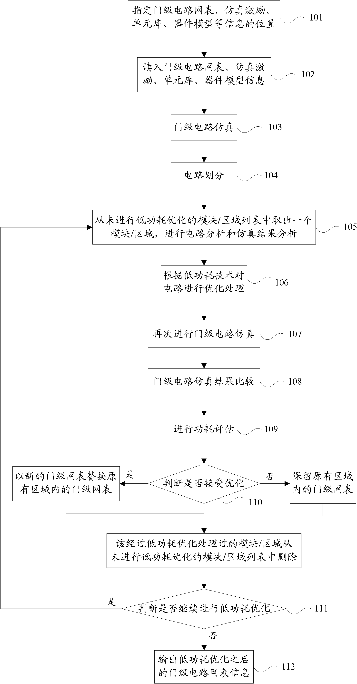
[0012] The present invention aims at optimizing the gate-level circuit netlist design, inserting and / or replacing some units in the circuit netlist to support MTCMOS, VTCMOS, power gating, multi-voltage, and dynamic voltage and frequency scaling (DVFS), power gating Low power consumption technology such as chip system makes the power consumption of the chip system the lowest under the premise of ensuring the circuit performance of the chip system.

[0013] In order to make the object, technical solution and advantages of the present invention clearer, the present invention will be further described in detail below in conjunction with the accompanying drawings.

[0014] figure 1 A flow chart of a method for optimizing a low-power circuit design provided by an embodiment of the present invention specifically includes the following steps:

[0015] Step 101, designate the location of gate-level circuit netlist, simulation stimulus, cell library, device model and other information...


PUM


Abstract

The invention discloses an optimization method of a low-power-consumption circuit design, belonging to the field of automation of integrated circuits. The optimization method comprises the following steps of: assigning positions of information of a gate-level circuit network table, simulation excitation, a unit library and a device model, reading the information in to execute the gate-level circuit simulation, partitioning gate-level circuits, executing circuit analysis and simulation result analysis, and executing optimization processing on the circuits according to the analysis results based on low-power-consumption technologies. According to the optimization method disclosed by the invention, the design of the gate-level circuit network table is optimized, and a part of units are inserted and/or replaced in the circuit network table to support the low-power-consumption technologies of an MTCMOS (Multi-threshold Complementary Metal Oxide Semiconductor), a VTCMOS (Variable Threshold Complementary Metal Oxide Semiconductor), power source gate control, multi-voltage and DVFS (Dynamic Voltage and Frequency Scaling), power gating d the like, thus the power consumption of a chip system is the minimum on the premise of ensuring circuit performances of the chip system.

Description

technical field [0001] The invention belongs to the field of integrated circuit design automation, in particular to the technical category of optimizing integrated circuit power consumption, in particular to a low-power consumption circuit design optimization method. Background technique [0002] The feature size of the advanced digital integrated circuit manufacturing process is continuously shrinking, from 90nm, 65nm, to 45nm, 32nm, and is expected to develop to 22nm and 15nm, or even smaller feature size. The continuous reduction of the feature size makes it possible to continuously improve the integration of the chip system, but the power consumption of the chip increases with the integration of the chip system, which restricts the ability to make full use of the reduction of the feature size to improve the integration of the chip system. Therefore, it is necessary to explore low-power optimization techniques to reduce the power consumption of the chip system. [0003] ...

Claims


Application Information

Patent Timeline
IPC IPC(8): G06F17/50
Inventor 吴玉平陈岚叶甜春
Owner INST OF MICROELECTRONICS CHINESE ACAD OF SCI
Why Eureka
Try Eureka