
Method for improving etching repeatability of gallium nitride (GaN) high electron mobility transistor (HEMT) grid trench

A repetitive, gate-groove technology, applied in semiconductor devices, electrical components, circuits, etc., can solve the problem of non-repetitive gate-groove etching, affecting the gate-groove etching rate, affecting the distance between the epitaxial wafer and the upper plate of the ICP cavity, etc. question

Active Publication Date: 2012-01-11
INST OF MICROELECTRONICS CHINESE ACAD OF SCI
View PDF1 Cites 2 Cited by
  • Summary
  • Abstract
  • Description
  • Claims
  • Application Information

AI Technical Summary

Problems solved by technology

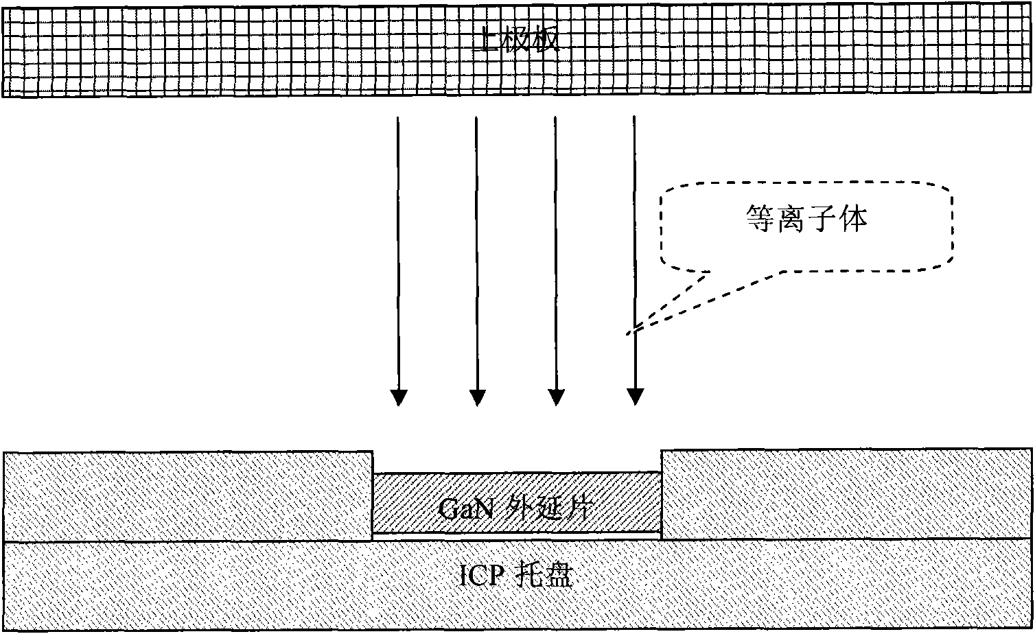
[0003] The gate groove etching process of GaN HEMT devices is very sensitive to the etching conditions. The thickness of the GaN epitaxial wafer will affect the distance between the epitaxial wafer and the upper plate of the ICP chamber, thereby affecting the gate groove etching rate.
Therefore, the thickness variation of different regions on the same GaN epitaxial wafer will cause uneven etching depth of the gate groove, and the thickness variation of different batches of GaN epitaxial wafers will cause non-repetition of the gate groove etching

Method used


Image

  • Method for improving etching repeatability of gallium nitride (GaN) high electron mobility transistor (HEMT) grid trench
  • Method for improving etching repeatability of gallium nitride (GaN) high electron mobility transistor (HEMT) grid trench
  • Method for improving etching repeatability of gallium nitride (GaN) high electron mobility transistor (HEMT) grid trench

Examples


Embodiment Construction

[0024] In order to make the object, technical solution and advantages of the present invention clearer, the present invention will be described in further detail below in conjunction with specific embodiments and with reference to the accompanying drawings.

[0025] Aiming at the etching damage and non-uniform and non-repetitive conditions in the traditional GaN HEMT gate groove etching process, the invention adopts a new type of ICP tray to reduce the etching damage and improve the etching uniformity and repeatability.

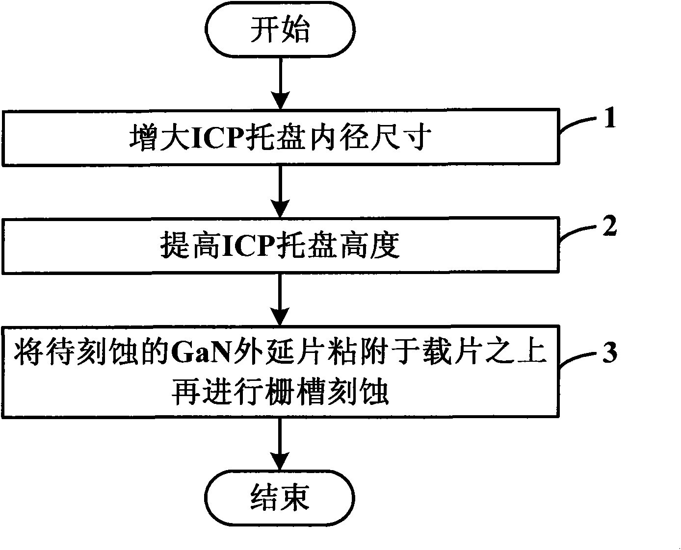
[0026] Such as figure 1 as shown, figure 1 It is a flowchart of a method for improving the repeatability of GaN HEMT gate groove etching provided by the present invention, the method includes:

[0027] Step 1: Increase the inner diameter of the ICP tray;

[0028] Step 2: Increase the height of the ICP tray;

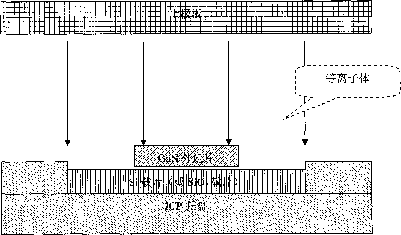
[0029] Step 3: Adhering the GaN epitaxial wafer to be etched on the carrier and then etching the gate groove.

[0030] Among them, increasing the in...


PUM


Abstract

The invention discloses a method for improving the etching repeatability of a gallium nitride (GaN) high electron mobility transistor (HEMT) grid trench. The method comprises the following steps of: enlarging the size of the inner diameter of an inductively coupled plasma (ICP) tray; increasing the height of the ICP tray; and bonding a GaN epitaxial slice to be etched on slide glass and etching the grid trench. By the method, the influence of the thickness of the GaN epitaxial slice on grid trench etching can be eliminated, the plasma bombardment damage during GaN HEMT grid trench etching is reduced and direct current and high frequency characteristics of a device can be improved by enlarging a plasma distribution volume in a reaction cavity body of an ICP etcher, reducing the density of plasmas and shortening an acceleration distance of the plasmas.

Description

technical field [0001] The invention relates to the technical field of semiconductor devices, in particular to a method for improving the repeatability of GaN HEMT gate groove etching. Background technique [0002] As a wide-bandgap compound semiconductor material device, GaN HEMT has the characteristics of high output power and high temperature resistance, and has broad application prospects. Gate trench etching technology, as an effective means to improve the transconductance of GaN HEMT devices and increase the power output, has been widely used in the production process of GaN HEMT devices. However, since the GaN cap layer that needs to be etched away is very thin, and the two-dimensional electron gas is also easily damaged by etching, this requires the gate groove etching to have the characteristics of shallow distance and low damage, and also requires good uniformity. and repeatability. [0003] The gate trench etching process of GaN HEMT devices is very sensitive to...

Claims


Application Information

Patent Timeline
IPC IPC(8): H01L21/335H01L21/28
Inventor 黄俊魏珂刘新宇刘果果樊捷
Owner INST OF MICROELECTRONICS CHINESE ACAD OF SCI
Learn More