Multi-input high-gain boost converter
A boost converter, high-gain technology, applied to conversion equipment without intermediate conversion to AC, photovoltaic power generation, etc., can solve the problems of complex structure, low work efficiency, and high cost of the rear-stage converter, and improve the overall work efficiency , Cost reduction, EMI small effect
- Summary
- Abstract
- Description
- Claims
- Application Information
AI Technical Summary
Problems solved by technology
Method used
Image
Examples
Embodiment 1
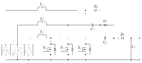
[0020] The input terminal of the second inductor L2 is connected to the positive pole of the second photovoltaic cell module, the output terminal is connected to one end of the second capacitor C2, and the other end of the second capacitor C2 is connected to the anode of the second diode D2; between the first capacitor C1 and The node of the first diode D1 is connected to the cathode of the second diode D2; the second power switch S2 is connected between the node of the second inductor L2 and the second capacitor C2 and the negative pole of the converter, and the second power switch S2 The source is connected to the negative pole of the converter, and the drain of the second power switch S2 is connected to the node;
[0021] The input terminal of the third inductor L3 is connected to the anode of the third photovoltaic cell module, and the output terminal is connected to the anode of the third diode D3; the junction of the second capacitor C2 and the second diode D2 is connecte...
Embodiment 2
[0031] According to the different states of the power switch, the circuit can be divided into 4 working states (taking the duty cycle of the first phase greater than the duty cycle of the second phase greater than the duty cycle of the third phase as an example):
[0032] (1) The controller controls the second power switch S2 to be turned off, and the first power switch S1 and the third power switch S3 to be turned on. At this time, the photovoltaic cell module 2 passes through the filter circuit, passes through the second inductor L2, the second capacitor C2 and the second The second diode D2 charges the first capacitor C1; at this time, both the first power switch S1 and the third power switch S3 are turned on, and the photovoltaic cell module 1 and the photovoltaic cell module 3 pass through their respective filter circuits and pass through the first power switch S1 and the third power switch S3 charge the first inductor L1 and the third inductor L3 respectively; the first d...
PUM
 Abstract
Description
Claims
Application Information
