Method for forming microelectro mechanical system (MEMS) device
A device and patterning technology, applied in the field of MEMS, can solve the problems of easy sliding of the film layer, difficult removal of the photoresist layer, and easy contamination of the chamber when the photoresist layer is removed. good compatibility
- Summary
- Abstract
- Description
- Claims
- Application Information
AI Technical Summary
Problems solved by technology
Method used
Image
Examples
Embodiment Construction
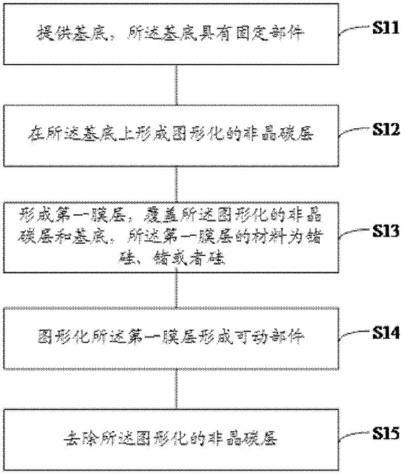
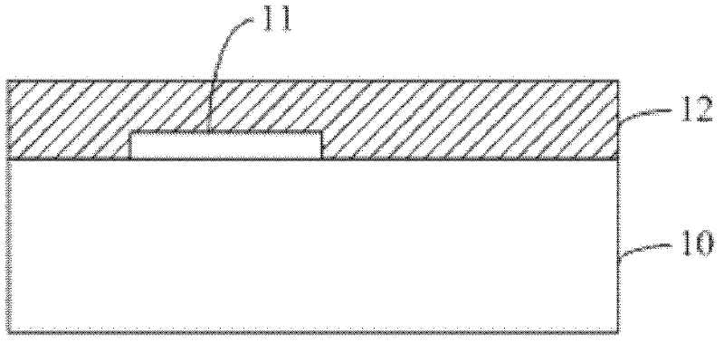
[0027] The method for forming a MEMS device according to a specific embodiment of the present invention uses amorphous carbon as a sacrificial layer to form a first film layer whose material is silicon germanium, germanium or silicon on the patterned amorphous carbon layer, and the first film layer after patterning Membranes serve as movable parts in MEMS devices.
[0028] In order to make the above objects, features and advantages of the present invention more comprehensible, specific implementations of the present invention will be described in detail below in conjunction with the accompanying drawings.
[0029] In the following description, specific details are set forth in order to provide a thorough understanding of the present invention. However, the present invention can be implemented in many other ways than those described here, and those skilled in the art can make similar extensions without departing from the connotation of the present invention. Accordingly, the p...
PUM
 Abstract
Description
Claims
Application Information
 - R&D
- Intellectual Property
- Life Sciences
- Materials
- Tech Scout
- Unparalleled Data Quality
- Higher Quality Content
- 60% Fewer Hallucinations
Browse by: Latest US Patents, China's latest patents, Technical Efficacy Thesaurus, Application Domain, Technology Topic, Popular Technical Reports.
© 2025 PatSnap. All rights reserved.Legal|Privacy policy|Modern Slavery Act Transparency Statement|Sitemap|About US| Contact US: help@patsnap.com


