Supercharge Your Innovation With Domain-Expert AI Agents!

Anti-NBTI (Negative-Bias Temperature Instability) effect reinforcing method based on CMOS (Complementary Metal-Oxide-Semiconductor Transistor) digital logic gate circuit

A digital logic and gate circuit technology, applied in logic circuits, electrical components, reliability improvement and modification, etc., can solve problems such as degradation effects, and achieve the effect of reducing increment and threshold voltage drift

Inactive Publication Date: 2012-01-25
SOUTH CHINA UNIV OF TECH
View PDF0 Cites 14 Cited by
  • Summary
  • Abstract
  • Description
  • Claims
  • Application Information

AI Technical Summary

Problems solved by technology

Although people have proposed many ways to weaken the NBTI effect at the circuit level, such as adjusting the power supply voltage, changing the input vector of the digital integrated circuit, adjusting the gate size, etc., for some circuits with specific requirements, the power supply voltage and input vector Both need to take a fixed value, and adjusting the gate size may cause other degradation effects, so these methods have certain limitations

Method used


Image

  • Anti-NBTI (Negative-Bias Temperature Instability) effect reinforcing method based on CMOS (Complementary Metal-Oxide-Semiconductor Transistor) digital logic gate circuit
  • Anti-NBTI (Negative-Bias Temperature Instability) effect reinforcing method based on CMOS (Complementary Metal-Oxide-Semiconductor Transistor) digital logic gate circuit
  • Anti-NBTI (Negative-Bias Temperature Instability) effect reinforcing method based on CMOS (Complementary Metal-Oxide-Semiconductor Transistor) digital logic gate circuit

Examples


Embodiment Construction

[0015] The specific implementation of the present invention will be further described below in conjunction with the accompanying drawings and examples, but the implementation and protection scope of the present invention are not limited thereto.

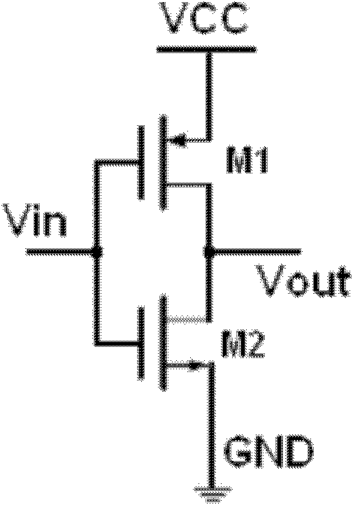
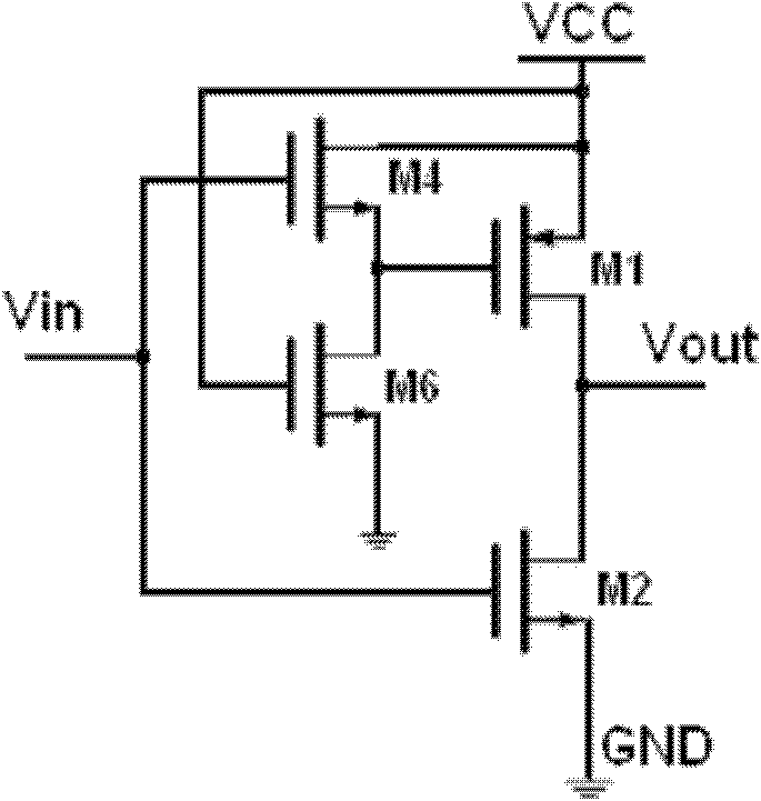
[0016] Such as Figure 1a For not using the common inverter circuit of the present invention, Figure 1b It is the embodiment circuit of the inverter of the present invention. exist Figure 1b In this embodiment, the input signal Vin is simultaneously connected to the gate of the second MOS transistor M2 and the gate of the fourth MOS transistor M4 of the source follower; the source output terminal of the fourth MOS transistor M4 is connected to the gate of the first MOS transistor M1 The gate of the sixth MOS transistor M6 is connected to VCC, the drain is connected to the source of the fourth MOS transistor M4, and the source is grounded, which is used as a current source load; the drains of the first MOS transistor M1 and the sec...


PUM


Abstract

The invention discloses an anti-NBTI (Negative-Bias Temperature Instability) effect reinforcing method based on a CMOS (Complementary Metal-Oxide-Semiconductor Transistor) digital logic gate circuit, which comprises the step of introducing a branch consisting of a source follower NMOS (N-channel Metal Oxide Semiconductor) transistor and a current source load NMOS transistor between an input node of the original CMOS digital logic gate circuit and a grid electrode of a PMOS (P-channel Metal Oxide Semiconductor) transistor, wherein the drain electrode of the source follower NMOS transistor is connected with a power supply, the grid electrode of the source follower NMOS transistor is connected with the input node of the logic gate circuit, the source electrode of the source follower NMOS transistor is connected with the grid electrode of the PMOS transistor; and the source electrode of the current source load NMOS transistor is grounded, the grid electrode of the current source load NMOS transistor is connected with the power supply, and the drain electrode of the current source load NMOS transistor is connected with the grid electrode of the PMOS transistor. Under the action of a source follower, the negative grid voltage of the PMOS transistor is reduced, the NBTI effect is weakened, and the drifting amount of the threshold voltage of the PMOS transistor and the circuit delay of the logic gate circuit are reduced. By using the anti-NBTI effect reinforcing method based on the CMOS digital logic gate circuit, the influence of the NBTI effect is minimized under a normal logic function, therefore, the anti-NBTI effect capacity of the CMOS digital integrated circuit is improved.

Description

technical field [0001] The invention relates to the technical field of CMOS integrated circuits, in particular to an anti-NBTI effect reinforcement method based on CMOS digital logic gates (inverters, NAND gates, and NOR gates) circuits. Background technique [0002] With the rapid development of the CMOS integrated circuit industry, the requirements for circuit reliability are getting higher and higher. The continuous reduction of feature size is one of the main directions of the development of the integrated circuit industry. However, the reduction in size will cause some degradation of device performance. The effect of negative bias temperature instability (NBTI: Negative Bias Temperature Instability) has become a key factor affecting the reliability of deep submicron CMOS integrated circuits. Explain that the holes in the inversion layer of PMOSFET devices are thermally excited under high-temperature negative gate voltage, and tunnel to silicon / silicon dioxide ( ) inte...

Claims


Application Information

Patent Timeline
IPC IPC(8): H03K19/003H03K19/0948
Inventor 李斌赵明剑刘利宁吴朝晖
Owner SOUTH CHINA UNIV OF TECH
Features
  • R&D
  • Intellectual Property
  • Life Sciences
  • Materials
  • Tech Scout
  • Unparalleled Data Quality
  • Higher Quality Content
  • 60% Fewer Hallucinations
Learn More