Defectivity-immune technique of implementing MIM-based decoupling capacitors

A capacitor and power supply decoupling technology, applied in the direction of electric solid-state devices, instruments, circuits, etc., can solve the problems of low defect rate, lower device output and/or reliability, etc.

Active Publication Date: 2012-02-01
AVAGO TECH WIRELESS IP SINGAPORE PTE
View PDF4 Cites 3 Cited by
  • Summary
  • Abstract
  • Description
  • Claims
  • Application Information

AI Technical Summary

Problems solved by technology

What these two implementations have in common is a small but non-negligible defect rate resulting in a low

Method used


Image

  • Defectivity-immune technique of implementing MIM-based decoupling capacitors
  • Defectivity-immune technique of implementing MIM-based decoupling capacitors
  • Defectivity-immune technique of implementing MIM-based decoupling capacitors

Examples


Embodiment Construction

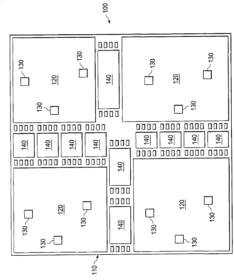
[0021] Using the gate dielectric layer as the capacitor dielectric, the defectivity of DECAP cells at the transistor layer is relatively low. This is because the decoupling capacitors are fabricated using the same processes used for standard CMOS transistors, which include high-quality gate dielectric layers. Therefore, the yield loss and / or current leakage of a design utilizing this DECAP is relatively low.

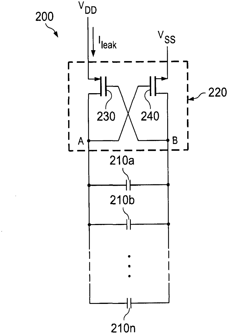
[0022] However, the interconnect layers used to form MiM-based DECAPs are generally more susceptible to processing defects that can lead to low-resistance paths (sometimes referred to herein as short circuits) between MiM DECAP levels. These deficiencies may reduce the overall yield and reliability of products utilizing the MiM DECAP. A short circuit through the MiM capacitor may cause a high current between the current source node and the ground node, thereby compromising the functionality of the entire device.

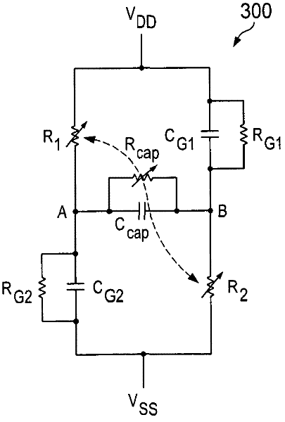
[0023] The present disclosure introduces a simple and n...


PUM


Abstract

The invention relates to a defectivity-immune technique of implementing MIM-based decoupling capacitors. An integrated circuit power supply decoupling circuit includes a capacitor and a protection circuit. The capacitor has a first terminal and a second terminal. The protection circuit includes a first transistor having a first conduction path, and a second transistor having a second conduction path. One terminal of the first conduction path is connected to the first terminal of the capacitor, and another terminal of the first conduction path is connected to a first power supply rail. One terminal of the second conduction path is connected to the second terminal of the capacitor, and another terminal of the second conduction path is connected to a second power supply rail.

Description

[0001] Cross References to Related Applications [0002] This application claims the benefit of U.S. Provisional Application No. 61 / 275,554, entitled "Defectivity-Immune Technique of Implementing MiM-Based Decoupling Capacitors," filed August 31, 2009 by Ramnath Venkatraman et al. commonly assigned and incorporated herein by reference. technical field [0003] This application relates generally to electronics and, more specifically, to power supply decoupling. Background technique [0004] Decoupling capacitors (DECAPs) are often incorporated into system-on-chip (SoC) designs to mitigate switching noise due to changes in current flowing through various parasitic inductances associated with the chip and the package in which the chip resides. Simultaneous switching of input / output (I / O) and core circuitry in the chip causes a voltage drop on the power supply of the order of ΔV=L(di / dt), where L is the effective wire inductance of the power bus (including the effective wire i...

Claims


Application Information

Patent Timeline
IPC IPC(8): H01L27/02H01L23/64H01L23/522
CPCH03K19/00346H01L2924/0002H01L2924/00G11C5/14G11C7/10
Inventor 拉纳思·温卡特拉曼鲁格罗·卡斯塔格内蒂
Owner AVAGO TECH WIRELESS IP SINGAPORE PTE
Why Eureka
Try Eureka