Sic semiconductor device

A semiconductor, conductive type technology, used in semiconductor devices, electrical components, circuits, etc., to solve problems such as insufficient contact

Active Publication Date: 2012-02-01
DENSO CORP +1
View PDF6 Cites 6 Cited by
  • Summary
  • Abstract
  • Description
  • Claims
  • Application Information

AI Technical Summary

Problems solved by technology

Thus, the contact between the contact area and the source electrode may not be sufficient

Method used


Image

  • Sic semiconductor device
  • Sic semiconductor device
  • Sic semiconductor device

Examples


no. 1 example

[0020] A MOSFET having an inversion type trench gate structure as an element in a SiC semiconductor device will be explained according to the first embodiment.

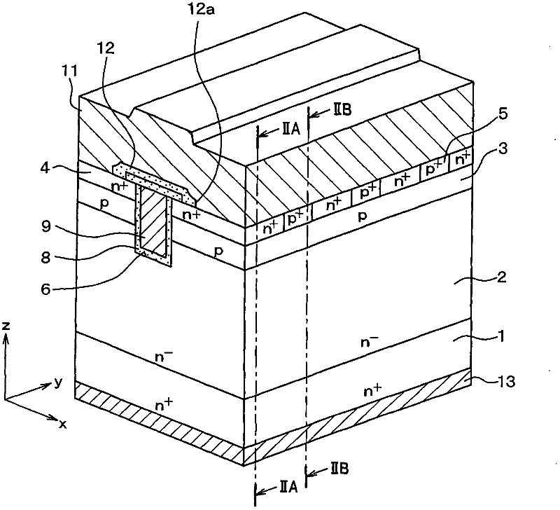
[0021] figure 1 A portion of a MOSFET according to the present embodiment is shown. figure 1 This part of the MOSFET corresponds to one cell of the MOSFET. In a MOSFET, multiple cells are arranged in a row, and each cell is shown in figure 1 middle. Figure 2A shows along the figure 1 A cross-sectional view of the MOSFET taken on line IIA-IIA, and this cross-sectional view is parallel to figure 1 X-Z plane in. Figure 2B shows along the figure 1 A cross-sectional view of the MOSFET taken on line IIB-IIB, and this cross-sectional view is parallel to figure 1 X-Z plane in. image 3 show figure 1 The upper layout view of the MOSFET in . figure 1 The MOSFET part corresponds to the image 3 District R in.

[0022] MOSFET consists of N made of SiC as the semiconductor substrate + Conductivity type substrate 1. ...

no. 2 example

[0037] In the SiC semiconductor device according to the second embodiment, on-resistance is improved.

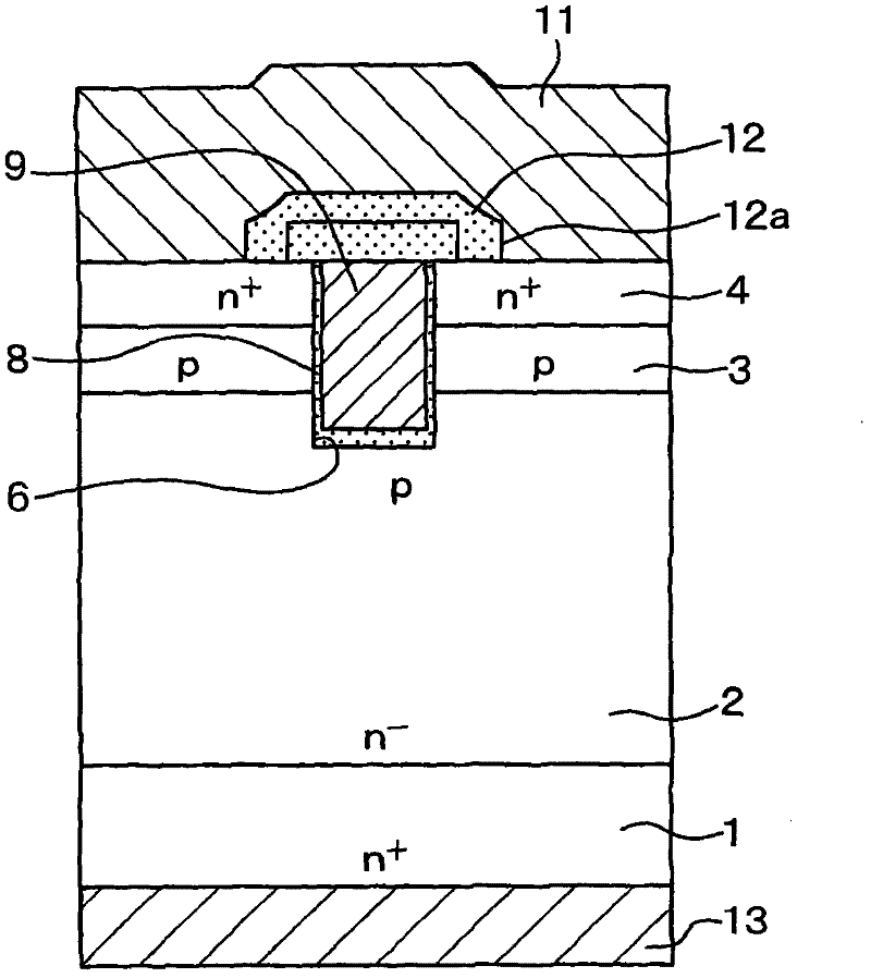
[0038] Figure 4 is a cross-sectional view of a MOSFET with a trench gate structure in a SiC semiconductor device. Figure 4 corresponds to Figure 2B . Figure 5 yes Figure 4 Top layout view of the MOSFET in .

[0039] The cross-sectional structure of the SiC semiconductor device according to this embodiment is similar to that of figure 1 in the structure.

[0040] Such as Figure 4 As shown in , in this embodiment, the body layer 5 forms a contact portion with the source electrode 11 . Body layer 5 is not formed on the entire sidewall of trench 6 so that body layer 5 is separated from trench 6 . Source region 4 is formed on the entire sidewall of trench 6 . Specifically, the body layer 5 sandwiches the trench gate structure via the source region 4 . A portion of source region 4 arranged on a line passing through body layer 5 and perpendicular to the longitudinal...

no. 3 example

[0043] The breakdown voltage of the SiC semiconductor device according to the third embodiment is improved.

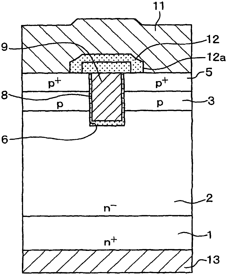
[0044] Figure 6 is a perspective view of a MOSFET having a trench gate structure in a SiC semiconductor device. Figure 7 yes Figure 6 Top layout view of the MOSFET in .

[0045] In the SiC semiconductor device, the deep layer 10 of the P conductivity type is formed in a part of the drift layer 2 disposed under the base region 3 and opposite to the body layer 5 . The deep layer 10 extends in a direction perpendicular to the longitudinal direction of the trench 6, and the extending direction of the deep layer 10 is the normal direction of the channel forming portion contacting the sidewall of the trench 6 (i.e., Figure 6 in the X direction). The deep layer 10 has a deeper depth than the bottom of the trench 6 . The depth of the deep layer 10 from the surface of the drift layer 2 is for example in the range between 2.6 micrometers and 3.0 micrometers such that th...


PUM


Abstract

A SiC semiconductor device includes a reverse type MOSFET having: a substrate 1; a drift layer 2 and a base region 3 on the substrate; a base contact layer 5 and a source region 4 on the base region; multiple trenches 6 having a longitudinal direction in a first direction penetrating the source region and the base region; a gate electrode 9 in each trench via a gate insulation film 8; an interlayer insulation film 12 covering the gate electrode and having a contact hole 12a, through which the source region and the base contact layer are exposed; a source electrode 11 coupling with the source region and the base region through the contact hole 12a; a drain electrode 13 on the substrate. The source region and the base contact layer extend along with a second direction perpendicular to the first direction, and are alternately arranged along with the first direction. The contact hole has a longitudinal direction in the first direction.

Description

technical field [0001] The present invention relates to SiC semiconductor devices including MOSFETs. Background technique [0002] Conventionally, Japanese Patent No. 3489358 teaches a SiC (ie, silicon carbide) semiconductor device having a vertical MOSFET as a vertical insulated gate type transistor. As shown in Figure 9A, in this device, the P coupled to the base region of P conductivity type + The longitudinal direction of the contact zone J2 of conductivity type is related to N + The longitudinal directions of the source region J1 of conductivity type and the base region of P conductivity type are parallel to the longitudinal direction of the trench J3, which provides a trench gate structure. The contact hole J4 formed in the interlayer insulating film is parallel to the longitudinal direction of the trench J3. N + conductivity type source regions J1 and P + A type of contact region J2 is electrically coupled with the source electrode through the contact hole. [0...

Claims


Application Information

Patent Timeline
Patent Type & Authority Applications(China)
IPC IPC(8): H01L29/78
CPCH01L29/1095H01L29/7828H01L29/0878H01L29/66068H01L29/0696H01L29/7397H01L29/1608H01L29/7813
Inventor 宫原真一朗高谷秀史杉本雅裕森本淳渡边行彦
Owner DENSO CORP
Why Eureka
Try Eureka