

Photoelectric conversion element, process for producing same, optical sensor, and solar cell
A technology of photoelectric conversion elements and photoelectrodes, applied in electrical components, capacitors, photovoltaic power generation, etc., can solve the problems of high power generation cost expansion, etc., and achieve the effect of excellent practicability
- Summary
- Abstract
- Description
- Claims
- Application Information
AI Technical Summary
Problems solved by technology
Method used
Image

Examples
Embodiment approach 1
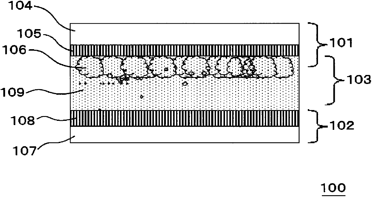
[0037] figure 1 is a sectional view showing the configuration of a photoelectric conversion element according to an embodiment of the present invention. figure 1 The photoelectric conversion element 100 shown in includes a photoelectrode 101 and a counter electrode (transparent electrode 107) arranged to face the photoelectrode 101, and the photoelectrode 101 includes a semiconductor layer (porous semiconductor layer 106) and a transparent conductive Substrate (transparent electrode 104). The photoelectrode 101 is formed of a substrate (transparent conductive substrate, transparent electrode 104 ) having a porous semiconductor layer 106 . Transparent electrodes 107 are stacked in such a manner as to face the photoelectrodes 101 .
[0038] As compounds having a light-absorbing function and a redox function, nitroxyl radical compounds having a 4,4,5,5-tetraalkylimidazoline-1-oxyl-3-oxide structure represented by general formula 1 mainly include between the photoelectrode 101 ...
Embodiment approach 2
[0095] According to the photoelectric conversion element 100 of Embodiment 1 ( figure 1 ) are well suited for use as, for example, dye-sensitized solar cells.
[0096] When sunlight is irradiated from the photoelectrode 101 side of the photoelectric conversion element 100, the sunlight sequentially passes through the transparent electrode 104 and the conductive layer 105, and irradiates a dye (not shown in the figure) absorbed on the porous semiconductor layer 106. The dye absorbs light and is thereby excited. Electrons generated by this excitation migrate from the porous semiconductor layer 106 to the conductive layer 105 . Electrons migrated to the conductive layer 105 migrate to the counter electrode 102 through an external circuit and return from the conductive layer 108 to the dye through the organic compound solution 109 . In this way, current flows to form a solar cell.
[0097] A plurality of photoelectric conversion elements according to the present invention can b...
Embodiment 1
[0116] A photoelectric conversion element according to the present invention was produced as follows. First, 5 g of commercially available titanium dioxide powder (product name: P25, manufactured by Nippon Aerosil Co., Ltd.), 20 mL of a 15% by volume acetate solution, 0.1 mL of a surfactant (product name : Triton X-100, manufactured by Sigma-Aldrich Co., Ltd.), and 0.3 g of polyethylene glycol (molecular weight: 20000) were stirred to prepare a titanium dioxide paste for forming a porous semiconductor layer.
[0117] Then, an appropriate amount (coating area: 3 cm x 3 cm) of titanium dioxide paste was coated on an ITO glass substrate (6 cm x 4 cm, sheet resistance: 20 Ω / □) to have a thickness of 20 μm using a doctor blade method. Here, the portion to which the paste was not applied was used as an electrode extraction portion and a sealing portion. Four through holes having 0.5 mmΦ were formed between the coating portion and the sealing portion. The electrode was inserted int...
PUM
| Property | Measurement | Unit |
|---|---|---|
| particle size | aaaaa | aaaaa |
| particle size | aaaaa | aaaaa |
Abstract
Description
Claims
Application Information