Fuse structure and method for forming the same

A fuse structure and fuse technology, which are applied in the manufacturing of electrical components, electric solid-state devices, semiconductor/solid-state devices, etc., can solve the problems of complex process, occupying COMS area, and small fusing current, so as to achieve a simple forming process and save chips. Area, the effect of reducing the manufacturing cost

Active Publication Date: 2012-02-08
XIAN YISHEN OPTOELECTRONICS TECH CO LTD
View PDF7 Cites 6 Cited by
  • Summary
  • Abstract
  • Description
  • Claims
  • Application Information

AI Technical Summary

Problems solved by technology

The first type of fuse structure directly uses the metal interconnection wire of the metal interconnection layer as the fuse, and uses laser to cut the fuse when repairing the circuit, so its cost is relatively high
The second type of fuse structure is in a programming circuit (one time programm, OTP), multiple programming circuit (multiple time programm, MTP) or electrically erasable programmable read-only memory (Electrically Erasable Programmable Read-Only Memory, EEPROM) The fuse structure used in the device is not stacked with OTP / MTP / EEPROM devices, which wastes chip area, and the process is complicated, resulting in high cost.
The third fuse structure is a polysilicon fuse structure, which uses a polysilicon gate in a CMOS (Complementary Metal Oxide Semiconductor) process as a fuse. Since polysilicon has a large resistance, its fusing current is small and will not Destroy the related circuit structure, but it occupies the CMOS area, thus increasing the manufacturing cost of semiconductor devices
Yet, all do not solve the shortcoming that exists in the above-mentioned prior art

Method used


Image

  • Fuse structure and method for forming the same
  • Fuse structure and method for forming the same
  • Fuse structure and method for forming the same

Examples


Embodiment Construction

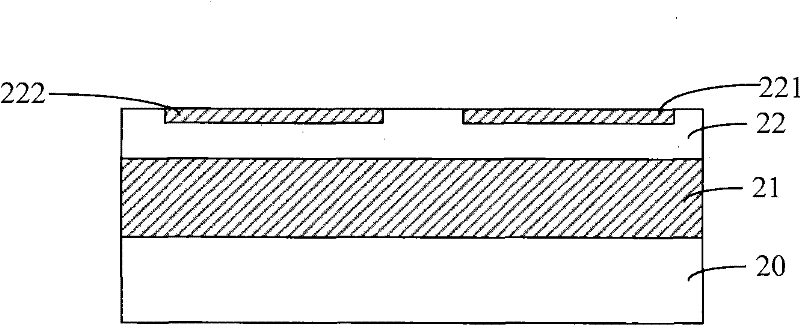
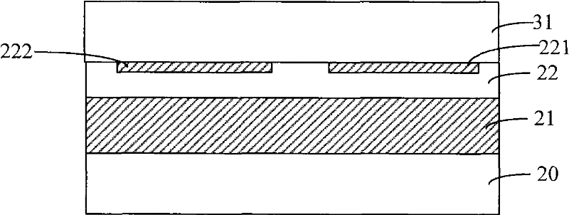
[0053] In the prior art, there is a fuse structure that uses polysilicon as a fuse. However, since the deposition temperature of polysilicon is above 600°C, it must be formed before the CMOS back-end process and is parallel to the CMOS circuit on the same plane. Therefore, the fuse structure It will occupy the area of ​​the chip and increase the cost. The inventor has repeatedly studied, hoping to find a fuse structure that can be formed after the CMOS back-end process and stacked on the CMOS circuit without occupying the chip area.

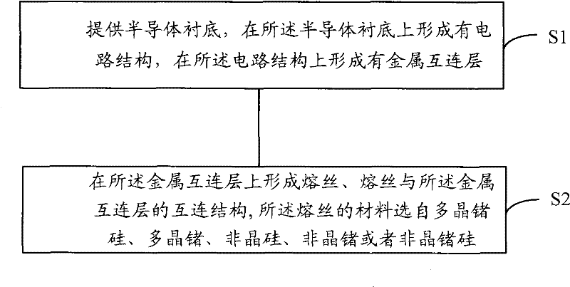
[0054] In the method for forming a fuse structure according to a specific embodiment of the present invention, after the circuit structure and the metal interconnection layer are formed, the interconnection structure of the fuse and the multi-fuse and the metal interconnection layer is formed on the metal interconnection layer.

[0055] In order to enable those skilled in the art to better understand the spirit of the present invention, the metho...


PUM

PropertyMeasurementUnit
thicknessaaaaaaaaaa

Abstract

A fuse structure and a method for forming the same are disclosed. The method is characterized in that: a semiconductor substrate is provided, wherein a circuit structure is formed on the semiconductor substrate and a metal interconnection layer is formed on the circuit structure; a fuse and an interconnection structure of the fuse and the metal interconnection layer are formed on the metal interconnection layer, wherein a material of the fuse is selected from polycrystalline germanium silicon, polycrystalline germanium, amorphous silicon, amorphous germanium or amorphous germanium silicon. Resistances of the polycrystalline germanium silicon, polycrystalline germanium, amorphous silicon, amorphous germanium or amorphous germanium silicon are high. When a polycrystalline germanium silicon fuse, a polycrystalline germanium fuse, an amorphous silicon fuse, an amorphous germanium fuse or an amorphous germanium silicon fuse are fused, a needed fusing current is small so that a relevant circuit structure is not easy to be destroyed. The fuse structure formed by using the method does not occupy a chip area when stacking on the metal interconnection layer. Therefore, the chip area can be saved and manufacturing costs can be reduced. A formation process is simple.

Description

technical field [0001] The invention relates to the technical field of semiconductors, in particular to a method for forming a fuse structure. Background technique [0002] Semiconductor integrated circuits include fuse structures, which are usually used in both circuit repair and changing the output logic value of a memory. In terms of circuit repair, when the circuit is repaired, the fuse connected to the faulty circuit is blown to make the faulty circuit structure unusable, and the faulty circuit is replaced with a redundant circuit. In terms of changing the output logic value of the memory, the output logic value is determined by blowing or not blowing the fuse. [0003] There are several common fuse structures in the prior art. The first type of fuse structure directly uses the metal interconnection wire of the metal interconnection layer as the fuse, and the fuse is cut off by laser when the circuit is repaired, so its cost is relatively high. The second type of fus...

Claims


Application Information

Patent Timeline
Patent Type & Authority Applications(China)
IPC IPC(8): H01L21/768H01L23/525
CPCH01L23/5256H01L2924/0002
Inventor 毛剑宏
Owner XIAN YISHEN OPTOELECTRONICS TECH CO LTD
Why Eureka
Try Eureka