Microelectronic acceleration sensor and manufacturing process thereof

A technology of acceleration sensor and preparation process, which is applied in the direction of measurement of acceleration, speed/acceleration/shock measurement, metal material coating technology, etc., and can solve the problem of inability to realize multi-threshold latch and threshold reading, and difficulty in improving chip performance and stability , complex sensor processing technology and other issues, to achieve the effect of realizing single-chip intelligence, simple and reliable process steps, and reducing size and cost

Inactive Publication Date: 2013-04-24
SOUTHEAST UNIV
View PDF5 Cites 0 Cited by
  • Summary
  • Abstract
  • Description
  • Claims
  • Application Information

AI Technical Summary

Problems solved by technology

However, since this type of acceleration sensor does not have a latch function, the power consumption of the system will be very high, especially in the case of long-term detection in the field environment, the power consumption problem will often become a crucial issue. The problem
The signal latch of the traditional MEMS acceleration sensor is generally implemented by a circuit, so the processing technology of the sensor is complicated and the cost is high
The traditional acceleration latch made by silicon micromachining technology can only realize single-threshold latching, and cannot realize multi-threshold latching and threshold reading. The important thing is that it uses SOI silicon wafers to make sensor chips, which not only costs more , and because the silicon structure layer is thin, it is difficult to improve the performance and stability of the chip

Method used


Image

  • Microelectronic acceleration sensor and manufacturing process thereof
  • Microelectronic acceleration sensor and manufacturing process thereof
  • Microelectronic acceleration sensor and manufacturing process thereof

Examples


Embodiment Construction

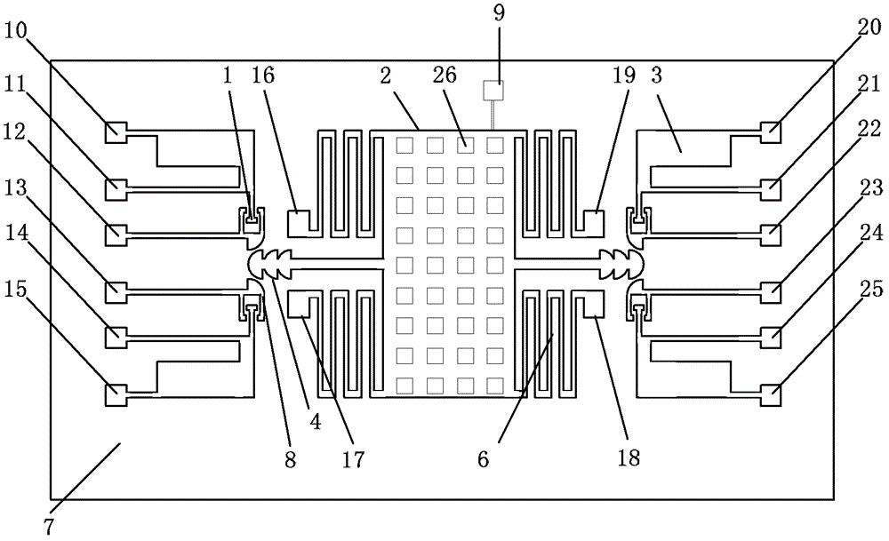
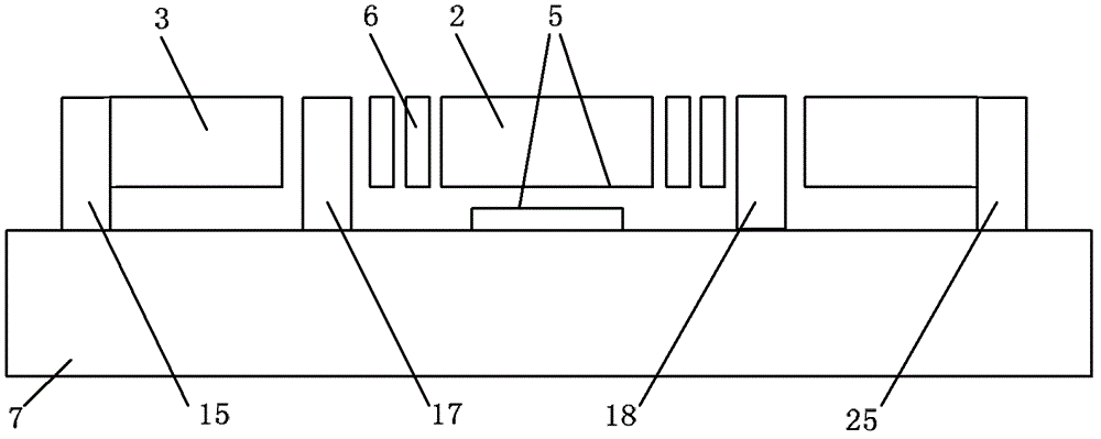
[0010] see figure 1 , 2 3, take the glass substrate 7 as the chip substrate, and set a single crystal silicon mass block 2 with a distance from the upper surface of the glass substrate 7 in the upper center of the upper surface of the glass substrate 7. There are square through holes 26 spaced apart and arranged in a rectangular array between the upper and lower surfaces of the mass block. Two monocrystalline silicon folding beams 6 are arranged symmetrically on the left and right sides, and the two monocrystalline silicon folding beams 6 on each side are symmetrically arranged on the upper and lower sides of the horizontal center line of the mass block, and one end of each monocrystalline silicon folding beam is respectively The suspension corresponds to the four symmetrical angles connecting the left and right of the mass block, and the other end of each single crystal silicon folded beam is respectively suspended and connected to the left and right two monocrystalline sili...


PUM

PropertyMeasurementUnit
lengthaaaaaaaaaa
widthaaaaaaaaaa
widthaaaaaaaaaa

Abstract

The invention discloses a microelectronic acceleration sensor. A monocrystalline silicon mass block which is separated from a glass substrate and is provided with a through hole is arranged above the glass substrate; four suspended folding beams are provided; one end of each of the four suspended folding beams is connected with four corners on the left side and the right side of the suspended mass block; the other ends of the four suspended folding beams are connected with four anchor areas which are symmetrically arranged on the left side and the right side; four suspended temperature-sensing beams are symmetrically arranged on the left side and the right side; each temperature-sensing beam is a bent beam with nonuniform thickness; the head end and the tail end of each temperature-sensing beam are connected with the respective anchor area of each temperature-sensing beam; suspended locking heads which have opposite directions and are horizontally arranged are connected at middle points of the left side and the right side of the suspended mass block; suspended locking hooks which are matched with the locking heads are arranged on the upper sides and the lower sides of the locking heads; the suspended locking hooks are connected with the respective anchor areas of the suspended locking hooks; a gold film layer is arranged on the upper surface of the glass substrate below the through hole of the suspended mass block; and all the anchor areas are rooted on the upper surface of the glass substrate. Through Au-Au low-temperature bonding, the bonding of monocrystalline silicon and the glass substrate and the electrical transfer and interconnection are realized.

Description

technical field [0001] The invention relates to a sensor microstructure for measuring acceleration based on micromachining, in particular to a microelectronic acceleration sensor and a preparation process thereof, belonging to the technical field of microelectromechanical systems. Background technique [0002] Acceleration is a very important parameter that reflects the external environment of the system and its own condition, and has an important impact on environmental monitoring and system self-state identification. Therefore, it is of great practical significance to quickly and accurately measure the acceleration. As we all know, although accelerometers using machining can also measure acceleration, these mechanical devices are easy to wear due to moving parts, and have the disadvantages of large size, high price, and frequent maintenance. A typical liquid-floating acceleration sensor has a large structure and relatively high power consumption. Micro inertial sensors ba...

Claims


Application Information

Patent Timeline
Patent Type & Authority Patents(China)
IPC IPC(8): G01P15/125B81C1/00
Inventor 秦明蔡春华
Owner SOUTHEAST UNIV
Why Eureka
Try Eureka