Nanometer multi-layer composite phase-change film material for multilevel storage phase-change memory, as well as preparation and application thereof

A composite phase change and nano-multi-layer technology, which is applied in the field of materials in the field of microelectronics technology, can solve the problems of data retention capacity decline, and achieve the effect of improving storage density, high data retention capacity, and good data retention capacity

Inactive Publication Date: 2012-02-15
TONGJI UNIV
View PDF2 Cites 14 Cited by
  • Summary
  • Abstract
  • Description
  • Claims
  • Application Information

AI Technical Summary

Problems solved by technology

Although Ge 2 Sb 2 Te 5 The performance of the film is balanced in all aspects, and there are no major shortcomings, but there are many areas worthy of improvement: First, like most phase change material systems, Ge 2 Sb 2 Te 5 The thin film only has high and low resistance states corresponding to logical "0" and "1", and there is a large room for improvement in storage density
Second, data retention needs to be improved, Ge 2 Sb 2 Te 5 The temperature at which the film can retain data for 10 years is around 80°C, and the data retention capability will drop sharply at higher temperatures

Method used


Image

  • Nanometer multi-layer composite phase-change film material for multilevel storage phase-change memory, as well as preparation and application thereof
  • Nanometer multi-layer composite phase-change film material for multilevel storage phase-change memory, as well as preparation and application thereof
  • Nanometer multi-layer composite phase-change film material for multilevel storage phase-change memory, as well as preparation and application thereof

Examples


Embodiment 1

[0036] Ge prepared in this example 2 Sb 2 Te 5 / Ga 30 Sb 70 The specific structure of the nanocomposite multilayer phase change film material is [Ge 2 Sb 2 Te 5 (33nm) / Ga 30 Sb 70 (67nm)] 1 、[Ge 2 Sb 2 Te 5 (40nm) / Ga 30 Sb 70 (60nm)] 1 、[Ge 2 Sb 2 Te 5 (50nm) / Ga 30 Sb 70 (50nm)] 1 、[Ge 2 Sb 2 Te 5 (60nm) / Ga 30 Sb 70 (40nm)] 1 and [Ge 2 Sb 2 Te 5 (67nm) / Ga 30 Sb 70 (33nm)] 1 , and the Ge 2 Sb 2 Te 5 / Ga 30 Sb 70 The total thickness of the nanometer multilayer composite phase change thin film material is 100nm.

[0037] The preparation steps are:

[0038] 1. Clean SiO2 2 / Si(100) substrate, cleaning the surface and back, removing dust particles, organic and inorganic impurities:

[0039] (a) strong ultrasonic cleaning in acetone solution for 3-5 minutes, rinse with deionized water;

[0040] (b) Strong ultrasonic cleaning in ethanol solution for 3-5 minutes, rinse with deionized water, high-purity N 2 Blow dry the surface and back;

[0041...

Embodiment 2

[0053] Ge prepared in this example 2 Sb 2 Te 5 / Ga 30 Sb 70 The specific structure of the nanocomposite multilayer phase change film material is [Ge 2 Sb 2 Te 5 (11nm) / Ga 30 Sb 70 (22nm)] 3 、[Ge 2 Sb 2 Te 5 (13nm) / Ga 30 Sb 70 (20nm)] 3 、[Ge 2 Sb 2 Te 5 (17nm) / Ga 30 Sb 70 (17nm)] 3 、[Ge 2 Sb 2 Te 5 (20nm) / Ga 30 Sb 70 (13nm)] 3 and [Ge 2 Sb 2 Te 5 (22nm) / Ga 30 Sb 70 (11nm)] 3 , and the Ge 2 Sb 2 Te 5 / Ga 30 Sb 70 The final sputtering total thickness of the nano-multilayer composite phase-change thin film material is controlled to be 100nm.

[0054] The preparation steps are:

[0055] 1. Clean SiO2 2 / Si(100) substrate, cleaning the surface and back, removing dust particles, organic and inorganic impurities:

[0056] (a) strong ultrasonic cleaning in acetone solution for 3-5 minutes, rinse with deionized water;

[0057] (b) Strong ultrasonic cleaning in ethanol solution for 3-5 minutes, rinse with deionized water, high-purity N 2 Blow dry...

Embodiment 3

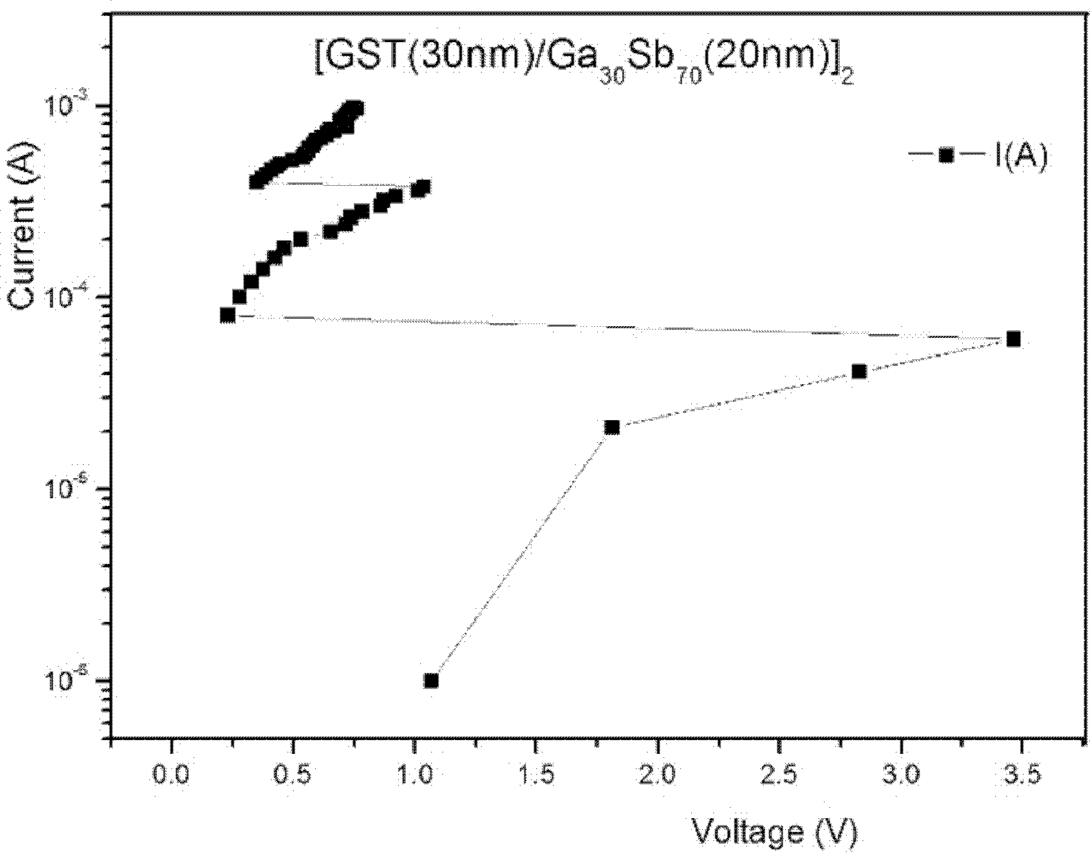
[0071] Ge prepared in this example 2 Sb 2 Te 5 / Ga 30 Sb 70 The specific structure of the nanocomposite multilayer phase change film material is [Ge 2 Sb 2 Te 5 (20nm) / Ga 30 Sb 70 (30nm)] 2 、[Ge 2 Sb 2 Te 5 (25nm) / Ga 30 Sb 70 (25nm)] 2 、[Ge 2 Sb 2 Te 5 (30nm) / Ga 30 Sb 70 (20nm)] 2 、[Ge 2 Sb 2 Te 5 (34nm) / Ga 30 Sb 70 (17nm)] 2 and [Ge 2 Sb 2 Te 5 (17nm) / Ga 30 Sb 70 (34nm)] 2 , and the Ge 2 Sb 2 Te 5 / Ga 30 Sb 70 The total thickness of the nanometer multilayer composite phase change thin film material is 100nm.

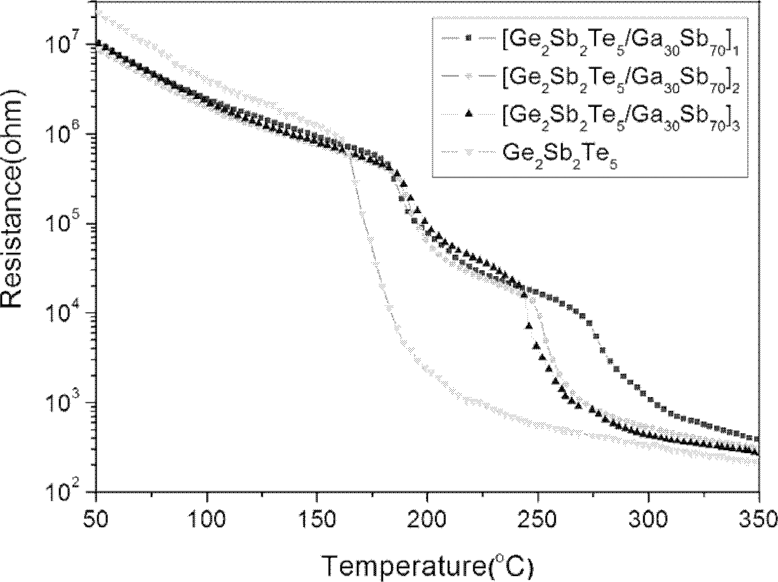
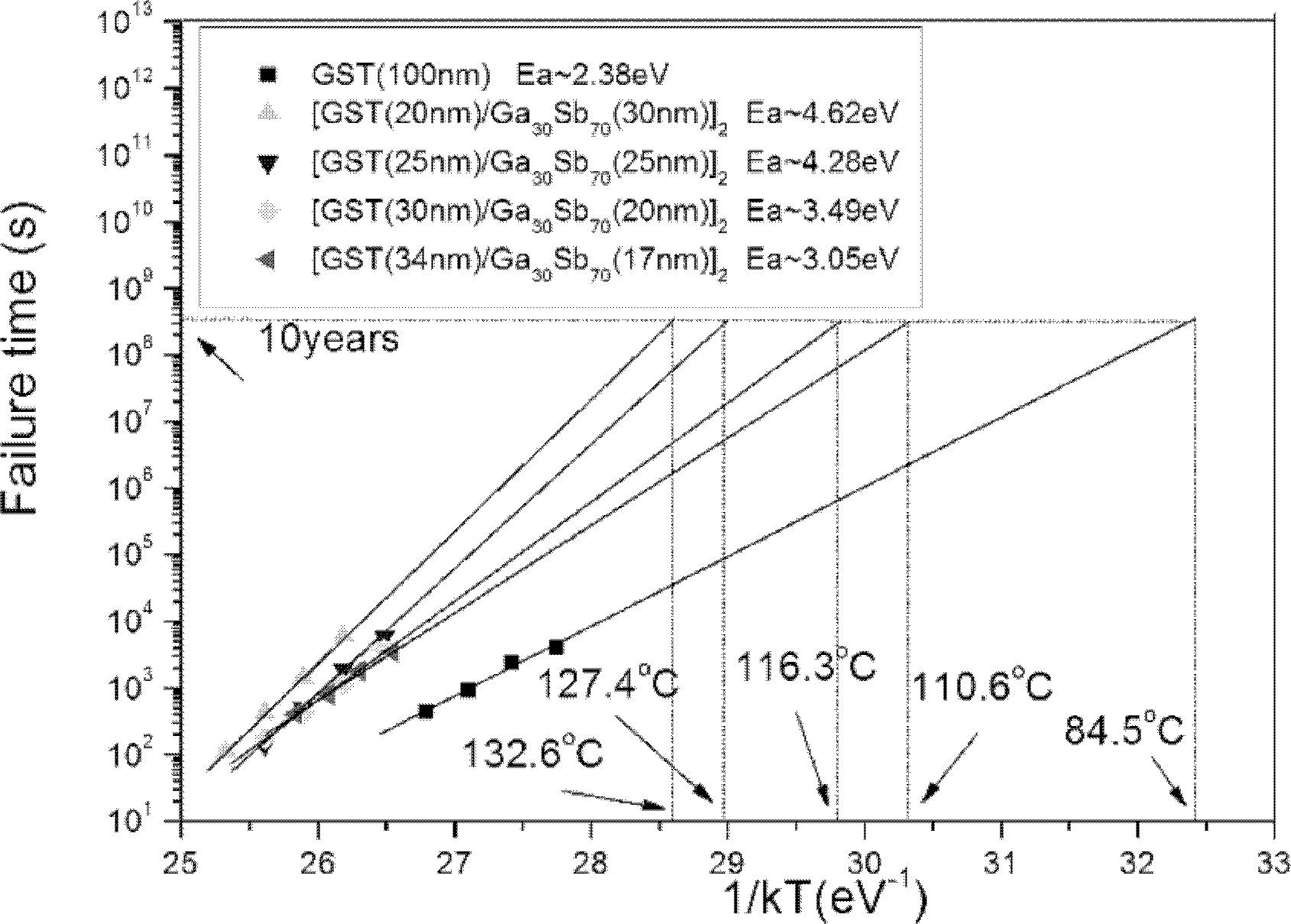
[0072] Each of the above 2 Sb 2 Te 5 / Ga 30 Sb 70 The preparation method of nanocomposite multilayer phase-change film material is identical with embodiment 2, and the final gained [Ge 2 Sb 2 Te 5 / Ga 30 Sb 70 ] 2 The total film thickness is 100nm, and the Ge 2 Sb 2 Te 5 with Ga 30 Sb 70 The thickness of the monolayer film is controlled by the difference of sputtering time.


PUM

PropertyMeasurementUnit
thicknessaaaaaaaaaa
thicknessaaaaaaaaaa
thicknessaaaaaaaaaa

Abstract

The invention relates to a Ge2Sb2Te5/Ga30Sb70 nanometer multi-layer composite phase-change film for a multilevel storage phase-change memory. A monolayer Ge2Sb2Te5 film and a monolayer Ga30Sb70 film in the Ge2Sb2Te5/Ga30Sb70 nanometer multi-layer composite phase-change film material are alternately ranged to form a multi-layer film structure, the thickness of the monolayer Ge2Sb2Te5 film and the thickness of the monolayer Ga30Sb70 film are respectively 10-133nm, and the total thickness of the Ge2Sb2Te5/Ga30Sb70 nanometer multi-layer composite phase-change film material is 90-200nm. When the Ge2Sb2Te5/Ga30Sb70 nanometer multi-layer composite phase-change film provided by the invention is applied to the phase-change memory, multilevel storage can be realized; and simultaneously, the Ge2Sb2Te5/Ga30Sb70 nanometer multi-layer composite phase-change film has higher heat stability and stronger data retention performance.

Description

technical field [0001] The invention relates to a material in the technical field of microelectronics, in particular to a Ge 2 Sb 2 Te 5 / Ga 30 Sb 70 Nano multilayer composite phase change thin film material. Background technique [0002] As a new generation of non-volatile memory technology, phase change memory (PCM) has the advantages of high reading and writing speed, high reliability, low power consumption, long life, high cycle times, and is compatible with COMS process (S . Lai and T. Lowrey: IEDM Tech. Dig., 2000, p. 243). Based on the above advantages, PCM has become the storage technology that is most likely to replace the currently commonly used FLASH technology and occupy the next-generation non-volatile storage market. PCM uses the Joule heat generated by the current to reversibly change the film resistance for programming. The film is amorphous at high resistance and crystalline at low resistance. The high and low resistance values ​​correspond to the logi...

Claims


Application Information

Patent Timeline
Patent Type & Authority Applications(China)
IPC IPC(8): H01L45/00B82Y30/00B82Y10/00B82Y40/00B32B9/00
Inventor 沈波孙明成翟继卫汪昌州
Owner TONGJI UNIV
Why Eureka
Try Eureka