Silicon-based coplanar micro-gas sensor chip and its application in micro-gas sensor preparation

A gas sensor and coplanar technology, applied in piezoelectric devices/electrostrictive devices, instruments, scientific instruments, etc., can solve the problems of poor sensor reliability and achieve high reliability, low production cost, and uniform temperature distribution

Inactive Publication Date: 2012-02-22
JILIN UNIV
View PDF4 Cites 16 Cited by
  • Summary
  • Abstract
  • Description
  • Claims
  • Application Information

AI Technical Summary

Benefits of technology

This technology allows for easy creation of small devices called sensors by making them more reliable at lower costs than traditional methods like thermocouple or resistance wire. These sensing elements are tiny parts on one side only, allowing it to measure temperatures up to 230°C without being affected by external factors such as pressure changes. They have strong connections between themselves but they cannot easily break down if bent too much force during use. Overall this design improves their durability over time while reducing overall productivity.

Problems solved by technology

This patented describes how current methods for making MEMS devices can be improved with smaller sizes while maintaining good electrical conductivity without increasing energy usage. One method involves creating tiny bending arms that block off some parts from being able to transmit thermal signals effectively. Another approach suggests placing these minute hotplates and signal elecrodes onto one side of the device instead of just overall improving its overall functionality through reduction of power consumed. Additionally, there may exist issues related to manufacturing stability during fabricating integrated circuits containing these components.

Method used


Image

  • Silicon-based coplanar micro-gas sensor chip and its application in micro-gas sensor preparation
  • Silicon-based coplanar micro-gas sensor chip and its application in micro-gas sensor preparation
  • Silicon-based coplanar micro-gas sensor chip and its application in micro-gas sensor preparation

Examples


Embodiment 1

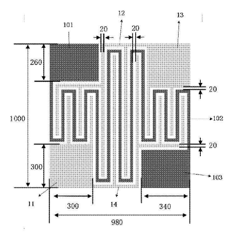
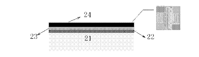
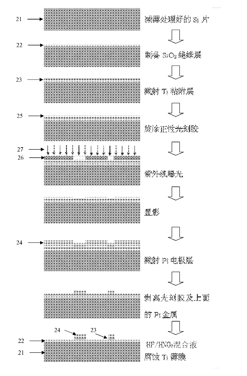
[0036] 1. Select the crystal orientation Si wafer, and reduce it as thin as possible under the condition of meeting the mechanical strength requirements of scribing. In this example, it is thinned to 300 μm; on one side of the thinned Si wafer Preparation of 300nm Thick SiO by Mixed Oxidation Method 2 Insulation layer; using semiconductor processing technology, in SiO 2 Sputter a 45nm-thick Ti adhesion layer on the insulating layer; spin-coat photoresist BP212 on the side of the Si wafer where metal Ti has been sputtered by using a homogenizer, the speed of the homogenizer is 3000r / min, and the homogenization time is 25s; After gluing, cover the glass mask on the Si wafer and align it, and expose it under 1000W optical power for 4s; use a positive photoresist developer to develop; sputter 250nm thick metal Pt on the photoresist-coated side of the developed Si wafer; Use the stripping process to strip the photoresist and the metal Pt on it; use HF:HNO 3 (molar ratio 4:1) the...


PUM

PropertyMeasurementUnit
Thicknessaaaaaaaaaa

Abstract

Belonging to the technical field of micro-nano electronic devices, the invention specifically relates to a silicon-based coplanar low-power micro-gas sensor chip and its application in micro-gas sensor preparation, wherein, the sensor chip is founded on a silicon substrate, and a heating electrode and a signal electrode coexist on one medium plane. And the prepared sensor of the above structure can realize operation at a low temperature. The micro-gas sensor chip is prepared by the steps of: preparing an SiO2 insulating layer on an Si substrate in (100) crystal orientation with a routine thermal oxidation method; employing a semiconductor plane technology to sputter a Ti adhesion layer and a Pt electrode layer (the heating electrode and the signal electrode) in order on the SiO2 insulating layer; then conducting photoetching and scribing so as to obtain a coplanar micro-gas sensor chip. The gas sensor chip prepared in the invention has low power consumption and is far superior to cantilever beam micro-sensors. The micro-gas sensor chip provided in the invention has the advantages of simple technology, low cost, low power consumption and easy integration.

Description


Claims


Application Information

Patent Timeline
Owner JILIN UNIV
Why Eureka
Try Eureka