Preparation method of photonic crystal multilayer film

A photonic crystal and multi-layer film technology, applied in coating, ion implantation plating, metal material coating process, etc., can solve the problems of high energy, less research, loss and so on

Inactive Publication Date: 2012-02-22
TAIYUAN UNIV OF TECH
View PDF5 Cites 4 Cited by
  • Summary
  • Abstract
  • Description
  • Claims
  • Application Information

AI Technical Summary

Problems solved by technology

[0004] The band gap structure of photonic crystals is the most important characteristic, and it is also the basis for the application and development of photonic crystals. The energy loss in the forbidden band of photonic crystals with multilayer film structure is low, but the forbidden band width is limited, and a wide full-angle height appears. Reflection is difficult; compa

Method used


Image

  • Preparation method of photonic crystal multilayer film
  • Preparation method of photonic crystal multilayer film
  • Preparation method of photonic crystal multilayer film

Examples


Embodiment Construction

[0068] The present invention will be further described below in conjunction with accompanying drawing:

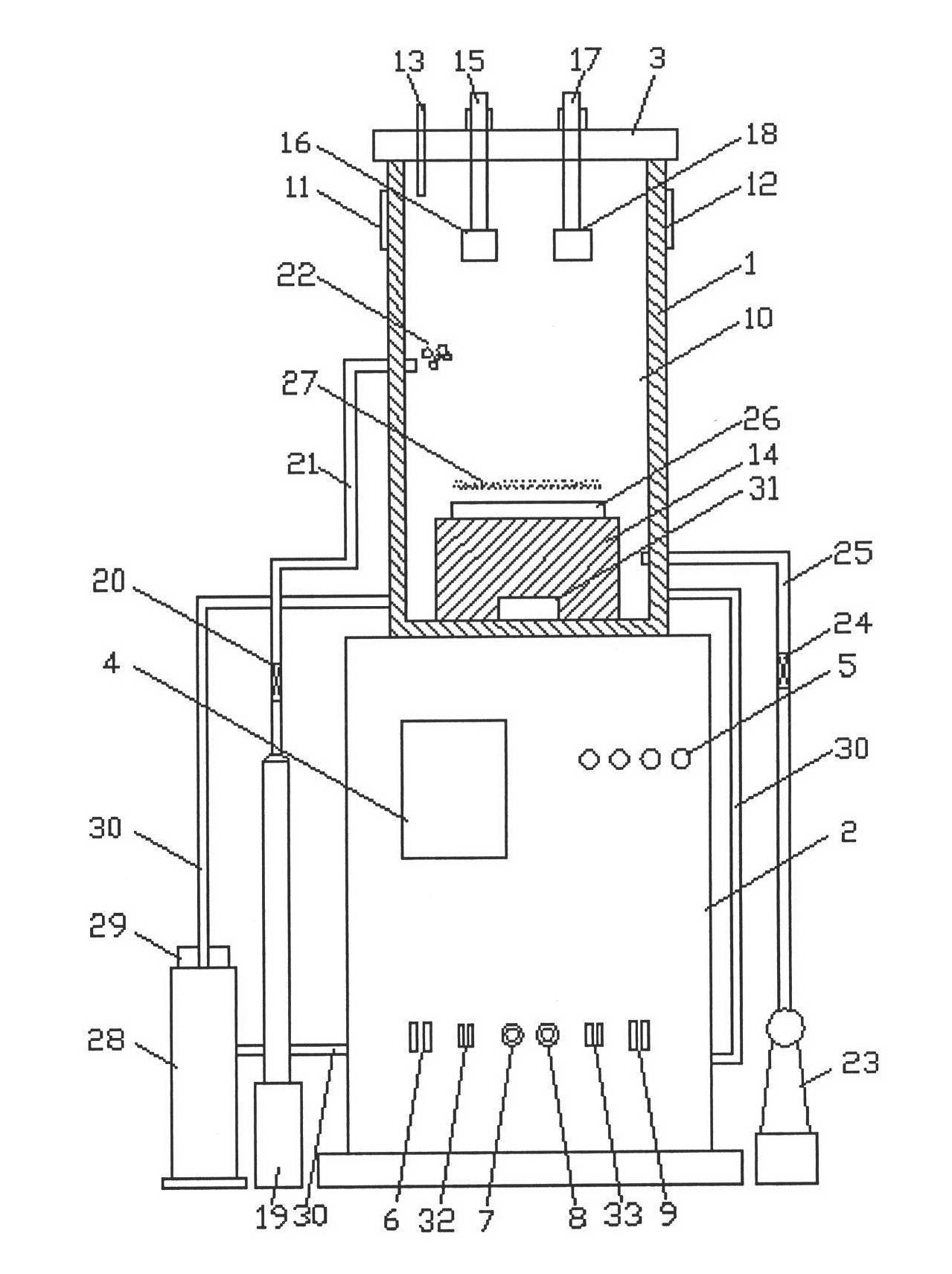
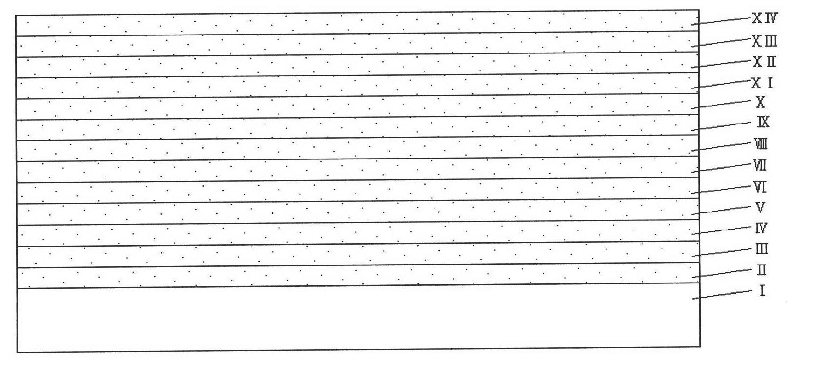
[0069] figure 1 As shown, it is the state diagram of photonic crystal multilayer film magnetron sputtering. The position and connection relationship of each part must be correct, and the ratio should be adjusted according to the quantity, and the operation should be performed in sequence.

[0070] The amount of chemical substances used in the preparation is determined according to the preset range in millimeters, milliliters, centimeters 3 is the unit of measurement.

[0071] The preparation of the photonic crystal multilayer film is carried out in a magnetron sputtering furnace. The lower part of the magnetron sputtering furnace 1 is a furnace base 2, and a display screen 4 and an indicator light 5 are arranged on the front control panel of the furnace base 2. , power switch 6, titanium oxide target source controller 7, copper target source controller 8, vacuum pump swit...


PUM


Abstract

The invention relates to a preparation method of a photonic crystal multilayer film. Aiming at application state of the photonic crystal to optical materials, an electrically conductive glass is used as a substrate, and titanium oxide and copper are used as films; TiO2 films and Cu films are sputtered on the substrate through magnetron sputtering; the TiO2 film and the Cu film alternatively arranged form a 14-layer multilayer film structure; then the multilayer film are treated with low temperature tempering to increase physical properties and mechanical properties of the multilayer film. Thepreparation method employs an advanced and rigorous technology with detailed and accurate technical parameters; the product has good quality, high purity and good optical performance; therefore, provided is an ideal preparation method of the photonic crystal multilayer film.

Description

technical field [0001] The invention relates to a method for preparing a photonic crystal multilayer film, which belongs to the technical field of preparation and application of optical materials. Background technique [0002] Photonic crystal is a new optical material that has appeared in recent years. It is an artificial crystal material composed of two materials with different dielectric parameters arranged periodically. It is the most promising new technology in the electronic information age since the application of electronic semiconductor materials. Material. [0003] Photonic crystals are mainly characterized by the existence of photonic band gap and photonic localization, and their characteristics enable photonic crystals to be applied in the integration of micro-optoelectronic devices, optical interconnection, and optical communication. [0004] The band gap structure of photonic crystals is the most important characteristic, and it is also the basis for the appli...

Claims


Application Information

Patent Timeline
IPC IPC(8): C23C14/35C23C14/14C23C14/08
Inventor 韩培德张雪张彩丽王丽萍张竹霞李玉平
Owner TAIYUAN UNIV OF TECH
Why Eureka
Try Eureka