
Method for forming resist pattern, and device

A resist pattern, resist technology, applied in the direction of photomechanical equipment, pattern surface photoengraving process, photoengraving process coating equipment, etc., can solve the problem of increasing developer consumption, increasing developer film thickness, etc. problem, to achieve the effect of reducing consumption and improving wettability

Inactive Publication Date: 2012-02-22
SEKISUI CHEM CO LTD
View PDF3 Cites 2 Cited by
  • Summary
  • Abstract
  • Description
  • Claims
  • Application Information

AI Technical Summary

Problems solved by technology

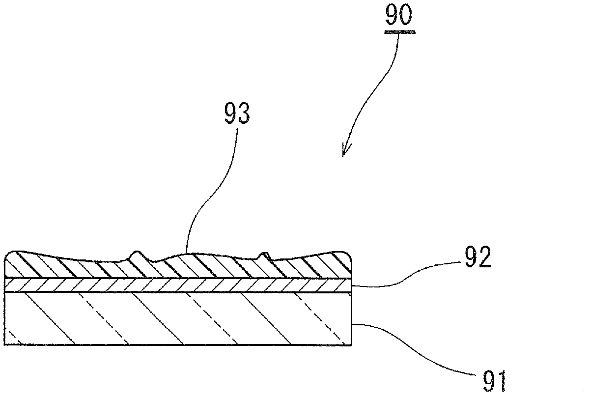
In particular, if the surface of the resist is uneven, it is necessary to increase the film thickness of the developer, and the consumption of the developer will increase.

Method used


Image

  • Method for forming resist pattern, and device
  • Method for forming resist pattern, and device
  • Method for forming resist pattern, and device

Examples


Embodiment 1

[0102] Examples will be described. It goes without saying that the present invention is not limited to this embodiment.

[0103] On the entire surface of the glass substrate 91, a positive resist is applied by slot coating and prebaked. The size of the glass substrate is 510 mm x 610 mm. The initial average thickness of the resist layer 93 is 500 nm. As the resist, ZEP520 manufactured by Nippon Zeon Co., Ltd. was used. The prebaking temperature was set at 150°C.

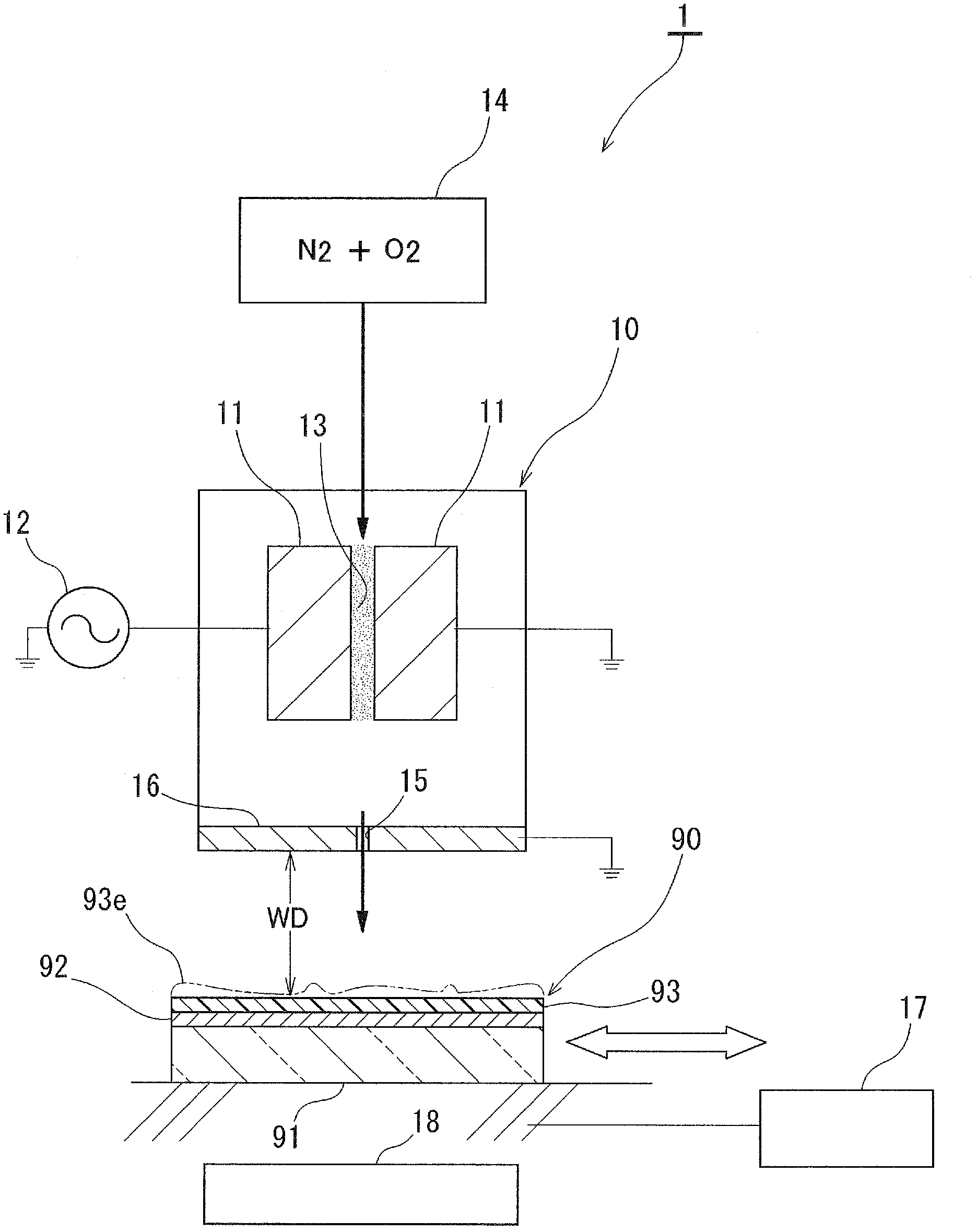
[0104] use with figure 2 or Figure 4 The atmospheric pressure remote plasma processing apparatuses 1 and 2 shown have substantially the same structure, and the atmospheric pressure remote plasma processing was performed on the above-mentioned sample. As a processing gas, a mixed gas of 600 L / min of nitrogen and 0.15 L / min of oxygen was used. The input power from the power source 12 to the electrode 11 was set to 3 kW. The transport speed by the moving mechanism 17 was set at 1.2 m / min. The number of times ...


PUM

PropertyMeasurementUnit
thicknessaaaaaaaaaa
thicknessaaaaaaaaaa

Abstract

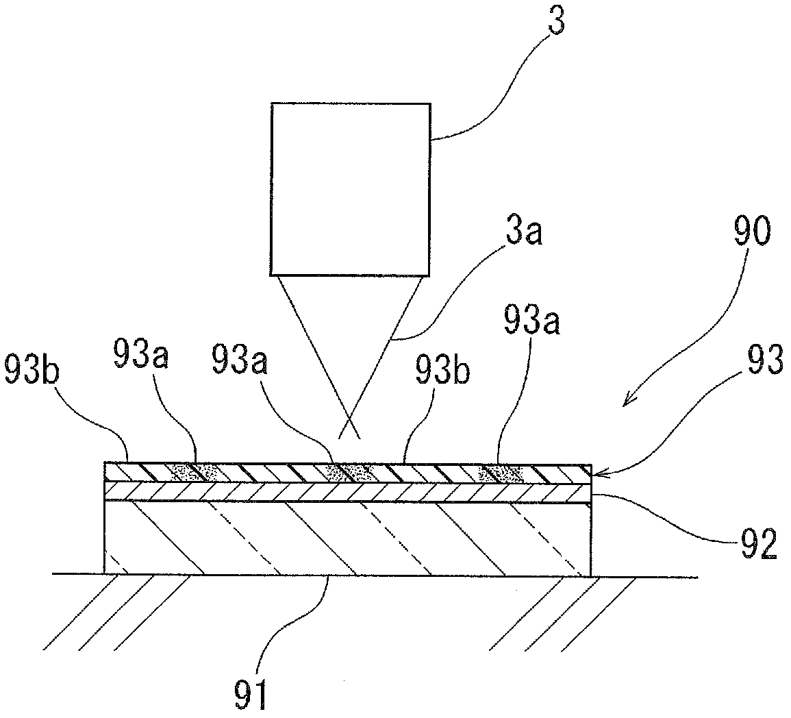
Disclosed is a method for forming a resist pattern, wherein the uniformity of development is improved by increasing the wettability of the surface of a resist layer when the resist pattern is formed on a device such as a photoresist. Specifically, a resist layer (93) is formed by applying a photosensitive resist over a substrate (91) (resist application step). Then, the resist layer (93) is partially irradiated with light (light exposure step). After that, a process gas for lyophilization is brought into contact with the resist layer (93) by being expelled through a discharge space (23) at near atmospheric pressure (atmospheric-pressure remote plasma lyophilization step). Then, a developer liquid (5) is brought into contact with the resist layer (93) (development step).

Description

technical field [0001] The present invention relates to a method of forming a resist pattern and a device manufactured by the method, and particularly to a method of forming a resist pattern suitable for manufacturing a photomask or a color filter as the above device. Background technique [0002] Photomasks are devices used in the manufacture of electronic components such as integrated circuits. Since the pattern of the photomask is copied onto the electronic component, whether the pattern is good or not has a great relationship with the quality of the electronic component. [0003] An example of the manufacturing process of a photomask is demonstrated. [0004] A light-shielding film made of chromium or the like is coated on the entire surface of the sufficiently cleaned glass substrate (light-shielding film forming step). On this light-shielding film, a photosensitive resist is applied by spin coating or slit coating (resist coating step). Resists can be classified as ...

Claims


Application Information

Patent Timeline
Patent Type & Authority Applications(China)
IPC IPC(8): G03F7/00G03F7/16G03F1/48H01L21/027G03F1/68G03F1/82G03F7/38
CPCG03F1/38G03F1/68
Inventor 上原刚青山哲平
Owner SEKISUI CHEM CO LTD
Learn More