Electroluminescence device

An electroluminescent device and light-emitting area technology, applied in electroluminescent light sources, electric light sources, lighting devices, etc., can solve problems such as examples that have not reported success

Inactive Publication Date: 2012-02-29
FUJIFILM CORP
View PDF5 Cites 0 Cited by
  • Summary
  • Abstract
  • Description
  • Claims
  • Application Information

AI Technical Summary

Problems solved by technology

However, no successful examples have been reported for EL devices

Method used


Image

  • Electroluminescence device
  • Electroluminescence device
  • Electroluminescence device

Examples


Embodiment Construction

[0033] Best Mode for Carrying Out the Invention

[0034] Embodiments of the present invention will now be described with reference to the accompanying drawings.

[0035]

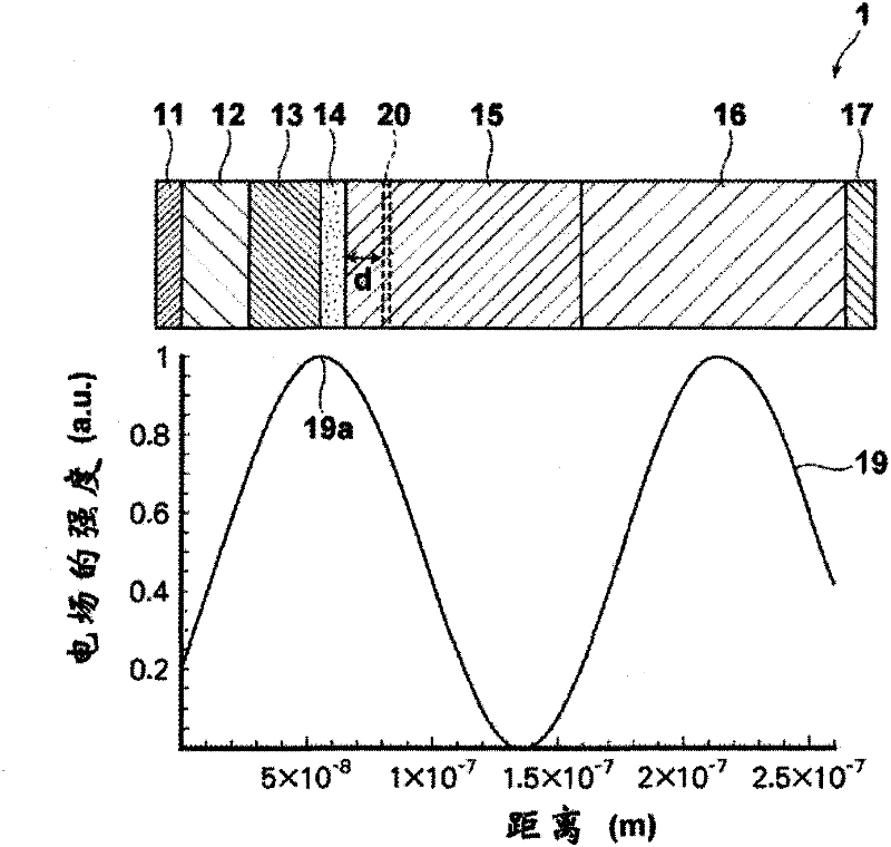
[0036] figure 1 is a schematic diagram illustrating the structure of the electroluminescence device (EL device) 1 according to the present embodiment. The EL device of the present embodiment is an organic EL device including a plurality of layers, and each layer thereof is formed of an organic layer.

[0037] The organic EL device 1 of the present invention has the structure of a common EL device, mainly comprising a cathode 11, an electron injection layer 12, an electron transport layer 13, a light emitting layer 14, a positive hole transport layer 15, a positive hole injection layer 16 and an anode 17. The light-emitting layer 14 is Alq3 in this example. When electrons and positive holes (holes) respectively injected from the cathode 11 and the anode 17 combine with each other at the region (light emi...


PUM


Abstract

An electroluminescence device (1) realizes high light emission efficiency, high durability, and high extraction efficiency. The device includes electrodes (11, 17); a plurality of layers (12 through 16) that are deposited between the electrodes (11, 17); and a light emitting region (14) between the plurality of layers (12 through 16). The light emitting region (14) emits light by application of an electric field between the electrodes (11, 17). The thickness and the refractive index of each of the plurality of layers (12 through 16) satisfy a resonance condition in the electroluminescence device (1) that makes a region in which the intensity of the electric field of a standing wave (19) by the light emitted from the light emitting region (14) is the highest substantially coincide with the light emitting region (14). A metal member (20) that induces plasmon resonance on the surface thereof by the emitted light is arranged in the vicinity of the light emitting region (14).

Description

technical field [0001] The present invention relates to an electroluminescent light-emitting device (electroluminescent device) that emits light by application of an electric field, and particularly to an electroluminescent device that can emit light with high efficiency. Background technique [0002] Electroluminescence devices (EL devices), such as organic EL devices, LEDs (Light Emitting Diodes) and semiconductor lasers are constructed in such a way that electrode layers, light emitting layers, etc. are deposited (stacked, overlapped, etc.) Wait. Generally, light generated in the light emitting layer is extracted through a transparent electrode. However, affected by the refractive index of each layer, when light enters the interface of the light extraction side layer at an angle greater than or equal to the critical angle, total reflection occurs. Therefore, light is trapped in the electroluminescent device, and light cannot be extracted therefrom. Therefore, efficient...

Claims


Application Information

Patent Timeline
Patent Type & Authority Applications(China)
IPC IPC(8): H01L51/50H05B33/22
CPCH10K50/11H10K50/852H10K50/858H01L2924/12044
Inventor 笠松直史
Owner FUJIFILM CORP
Why Eureka
Try Eureka