Precleaning process of silicon wafer

A technology for pre-cleaning and silicon wafers, applied in cleaning methods and utensils, sustainable manufacturing/processing, cleaning methods using liquids, etc., can solve the problem of large amount of hydrogen peroxide, unstable hydrogen peroxide, poor cleaning effect, etc. problems, to achieve high yield, high photoelectric conversion efficiency, and low surface tension

Inactive Publication Date: 2012-03-07
ZHEJIANG BEYONDSUN PV
View PDF5 Cites 13 Cited by
  • Summary
  • Abstract
  • Description
  • Claims
  • Application Information

AI Technical Summary

Problems solved by technology

[0004] The Chinese patent No. 201010618904 discloses a pre-cleaning process, which uses a cleaning solution composed of strong alkali, hydrogen peroxide and water to clean silicon wafers. However, in a strong alkali environment, hydrogen peroxide is unstable and decomposes The speed is extremely fast, resulting in poor cleaning effect in the later production, and the amount of hydrogen peroxide is huge, and the cost is high

Method used


Image

  • Precleaning process of silicon wafer
  • Precleaning process of silicon wafer
  • Precleaning process of silicon wafer

Examples


Embodiment 1

[0024] a) Immersion treatment, put the silicon wafer into the immersion solution, heat the immersion solution to 75°C, and immerse for 600s, wherein the immersion solution includes isopropanol accounting for 6% of the total volume and additives accounting for 8‰ of the total volume;

[0025] b) Rinse once, use deionized water to rinse the silicon wafer after soaking, the rinse time is 300s, and the temperature of deionized water is 70°C;

[0026] c) Oxidation treatment, put the silicon wafer rinsed once into the oxidizing solution, heat the oxidizing solution to 59°C, and oxidize for 500 seconds, wherein the oxidizing solution includes ammonia water accounting for 5% of the total volume, and ammonia water accounting for 8% of the total volume. Hydrogen peroxide, the rest is water;

[0027] d) Second rinse, using deionized water to rinse the oxidized silicon wafer for 300s, wherein the temperature of the deionized water is 70°C.

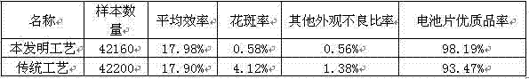
[0028] Through actual operation, the process o...

Embodiment 2

[0031] a) Immersion treatment, put the silicon wafer into the immersion solution, heat the immersion solution to 55°C, and immerse for 200s, wherein the immersion solution includes isopropanol accounting for 2% of the total volume and additives accounting for 2‰ of the total volume;

[0032] b) Rinse once, use deionized water to rinse the silicon wafer after soaking, the rinse time is 100s, and the temperature of deionized water is 40°C;

[0033] c) Oxidation treatment, put the silicon wafer rinsed once into the oxidizing solution, heat the oxidizing solution to 50°C, and oxidize for 200s, wherein the oxidizing solution includes 2% of the total volume of ammonia water, 3% of the total volume of Hydrogen peroxide, the rest is water;

[0034] d) Second rinse, using deionized water to rinse the oxidized silicon wafer for 100s, wherein the temperature of the deionized water is 40°C.

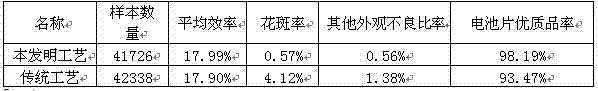
[0035] Through actual operation, the process of the present invention compares with traditional ...

Embodiment 3

[0039] a) Immersion treatment, put the silicon wafer into the immersion solution, heat the immersion solution to 60°C, and immerse for 400s, wherein the immersion solution includes isopropanol accounting for 4% of the total volume and additives accounting for 6‰ of the total volume;

[0040] b) Rinse once, use deionized water to rinse the silicon wafer after soaking, the rinse time is 200s, and the temperature of deionized water is 55°C;

[0041] c) Oxidation treatment, put the silicon wafer rinsed once into the oxidizing solution, heat the oxidizing solution to 55°C, and oxidize for 340s, wherein the oxidizing solution includes 4% of the total volume of ammonia water, 5% of the total volume of Hydrogen peroxide, the rest is water;

[0042] d) Second rinse, using deionized water to rinse the oxidized silicon wafer, the rinse time is 200s, wherein the temperature of the deionized water is 56°C.

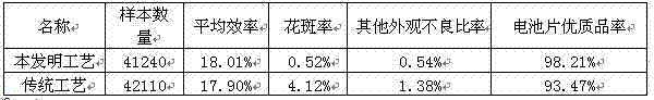
[0043] Through actual operation, the process of the present invention compares wi...


PUM


Abstract

The invention relates to a precleaning process of a silicon wafer, which comprises the following step of: precleaning the silicon wafer by sequentially performing procedures of soaking treatment, primary rinsing, oxidation treatment and secondary rinsing. In the oxidation process, the decomposition rate of hydrogen peroxide can be controlled in an alkalescence environment, the amount of the used hydrogen peroxide is reduced on the basis of not influencing the oxidation effect, and the cost is greatly reduced; in addition, in the oxidation process, a large amount of bubbles cannot be generatedin the decomposition process of the hydrogen peroxide, and the silicon wafer can be prevented from floating; and therefore the precleaning process disclosed by the invention is completely reliable and is high in finished product rate.

Description

technical field [0001] The invention relates to a silicon chip pre-cleaning process, which is used for making monocrystalline silicon solar cells, and belongs to the technical field of solar cell production technology. Background technique [0002] In the production of monocrystalline cells, the mottling rate of cell appearance caused by white spots and fingerprints is relatively high, which seriously affects the company's production cost and market competitiveness. [0003] Through a large number of experiments, it is concluded that the formation of white flakes and fingerprints is caused by poor incoming materials on the one hand, that is, the surface attachments of incoming silicon wafers, such as organic matter, oil, cleaning agent residue, silica gel, glove sweat residue, etc.; on the other hand, it is caused by Caused by abnormalities in the process, such as manual contact. Therefore, pre-cleaning is required before incoming silicon wafers are produced. [0004] The ...

Claims


Application Information

Patent Timeline
Patent Type & Authority Applications(China)
IPC IPC(8): H01L21/02H01L31/18B08B3/08
CPCY02P70/50
Inventor 王虎靳建光查达其姚琪陆波
Owner ZHEJIANG BEYONDSUN PV
Why Eureka
Try Eureka