Low power consumption weak signal amplification shaping circuit

A weak signal amplification and shaping circuit technology, applied in the direction of pulse shaping, etc., can solve the problems of large current consumption, very sensitive changes, and changes in the duty cycle of the output square wave signal in the amplifying circuit, and achieve the effect of ensuring accuracy

Active Publication Date: 2012-03-07
INST OF ELECTRONICS CHINESE ACAD OF SCI
View PDF3 Cites 6 Cited by
  • Summary
  • Abstract
  • Description
  • Claims
  • Application Information

AI Technical Summary

Problems solved by technology

In order to achieve such a high magnification, the amplifying circuit needs to consume a large amount of current
In addition, the change of the flipping threshold will lead to the cha

Method used


Image

  • Low power consumption weak signal amplification shaping circuit
  • Low power consumption weak signal amplification shaping circuit
  • Low power consumption weak signal amplification shaping circuit

Examples


Embodiment Construction

[0038] The technical solution of the present invention will be described in detail below in conjunction with the accompanying drawings.

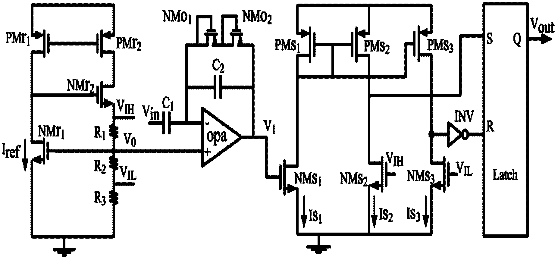
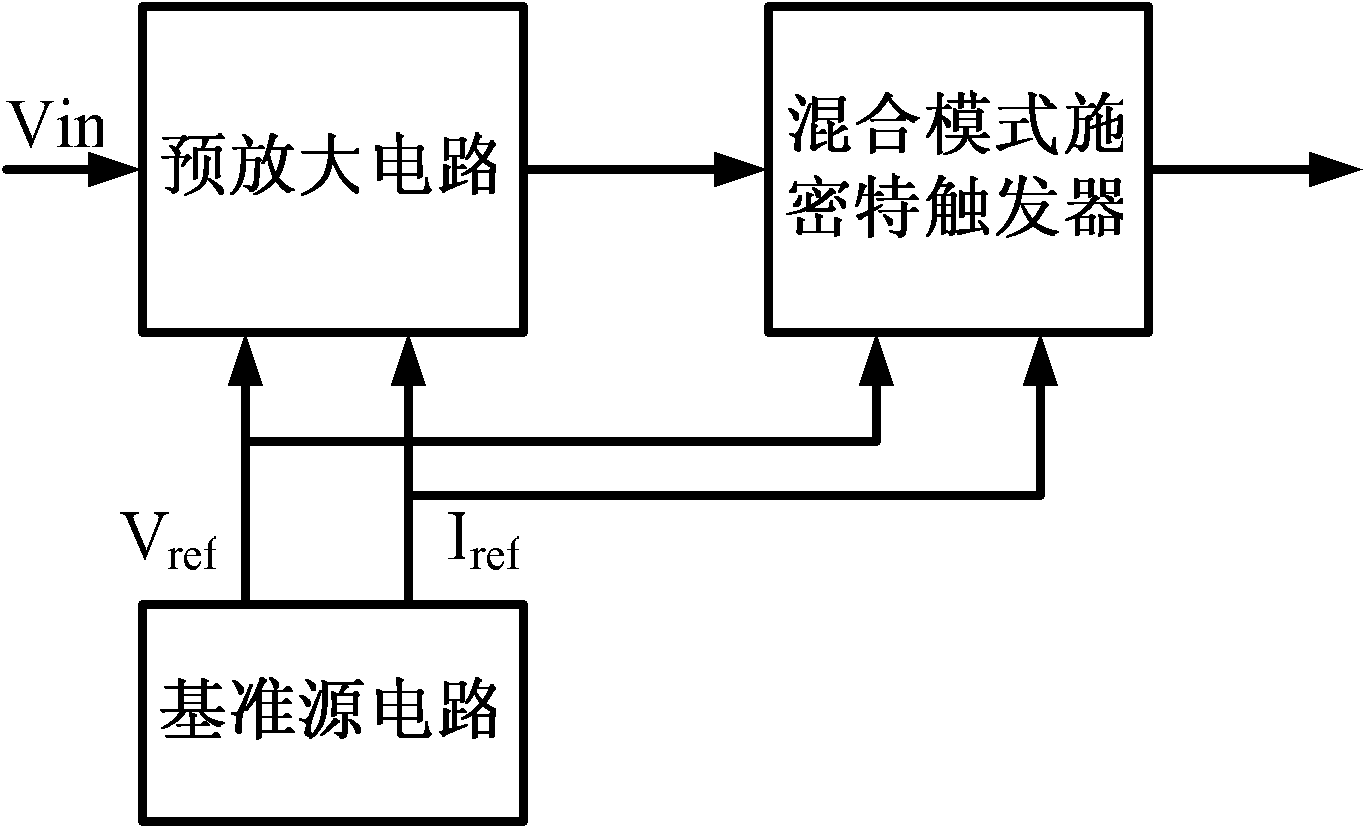
[0039] figure 1 The system structure diagram of the amplification and shaping circuit for weak signals. The whole system is mainly composed of three modules: a reference source circuit module, an amplifier circuit module, and a mixed-mode Schmitt trigger module. The reference circuit provides current and voltage references for other modules. The amplifying circuit amplifies the weak input signal, and the mixed-mode Schmitt trigger shapes the amplified signal to obtain an ideal full-scale output square wave signal.

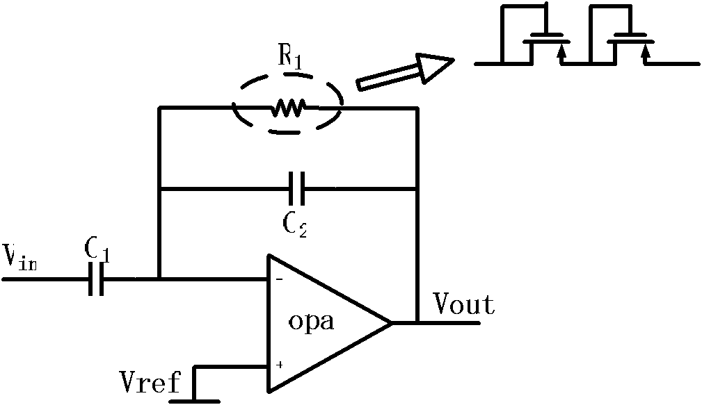
[0040] figure 2 Shown is the schematic diagram of the amplifier circuit. This structure can prevent the DC offset introduced by the previous circuit, and has the advantages of low power consumption. Its magnification is

[0041] G = 1 jw ...


PUM


Abstract

The invention discloses a low power consumption weak signal amplification shaping circuit, which relates to the technology of integrated circuits and comprises a reference source circuit, an amplification circuit and a Schmitt trigger shaping circuit, wherein the amplification circuit consists of an opa (optoelectronic pulse amplifier), two capacitors and two PMOS (positive channel metal oxide semiconductor) tubes, the Schmitt trigger shaping circuit consists of three PMOS tubes, three NMOS (N-Metal-Oxide-Semiconductor) tubes, an inverter INV and an SR (Synchronous Reset) trigger, and the reference source circuit consists of two PMOS tubes, two NMOS tubes and three resistors. In the invention, a flip threshold controllable mixed mode Schmitt trigger is adopted, and three equally-spaced negative temperature coefficient reference voltage offset pre-amplification circuits and Schmitt triggers are used so as to ensure the circuit of higher precision under any PVT (process verification test) conditions. The circuit disclosed by the invention has lower power consumption, and simultaneously has higher PVT change resisting capacity.

Description

technical field [0001] The invention relates to the technical field of integrated circuits, and is a weak signal amplification and shaping circuit with low power consumption, which amplifies and shapes weak signals such as square waves and sine waves into full-scale square waves. Background technique [0002] With the rapid development of the integrated circuit manufacturing industry, high density, high performance, low cost, and low power consumption have become the main trend of integrated circuit design development. With the gradual popularization of wireless mobile technology, the design requirement of low power consumption has become particularly urgent. [0003] Signals on the order of millivolts and below are called weak signals. Weak signal amplification and shaping circuits are widely used in systems such as biological signal acquisition, RFID, wireless electronic charging, wireless sensor networks, and the Internet of Things. For example, in the highway wireless ...

Claims


Application Information

Patent Timeline
IPC IPC(8): H03K5/02
Inventor 朱文锐杨海钢张丹丹支天程小燕
Owner INST OF ELECTRONICS CHINESE ACAD OF SCI
Why Eureka
Try Eureka