Semiconductor Wafer Cooling Device
A cooling device and semiconductor technology, applied in the manufacture of semiconductor/solid-state devices, discharge tubes, electrical components, etc., can solve problems such as temperature difference, deviation of electrical characteristics of the life of semiconductor components, etc., to suppress temperature difference, suppress temperature unevenness, close contact sex-enhancing effect
- Summary
- Abstract
- Description
- Claims
- Application Information
AI Technical Summary
Problems solved by technology
Method used
Image

Examples
Embodiment approach 1
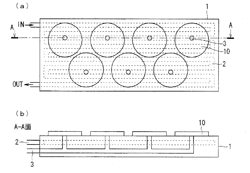
[0038] figure 1 is a block diagram of a semiconductor wafer cooling device according to Embodiment 1, figure 1 (a) is a plan view, figure 1 (b) is figure 1 A-A section view in (a).
[0039] In the semiconductor wafer cooling device of the present embodiment, a plurality of semiconductor wafers 10 are placed on the tray 1 on the placement surface thereof. A cooling duct 2 is formed inside the tray 1 , and the semiconductor wafer 10 is cooled by a cooling medium such as cooling water flowing through the cooling duct 2 . For example, cooling duct 2 such as figure 1 As shown in (a), one cooling duct is arranged in a folded shape (serpentine arrangement) between both ends of the tray 1 .
[0040] Furthermore, a vacuum duct 3 is formed inside the tray 1 so as not to interfere with the cooling duct 2 , and an opening of the vacuum duct 3 is formed on the mounting surface of the tray 1 . The inside of the vacuum duct 3 is depressurized by a vacuum pump, and the semiconductor waf...
Embodiment approach 2
[0046] figure 2 It is a block diagram of the semiconductor wafer cooling apparatus of Embodiment 2. In the semiconductor wafer cooling device of this embodiment, a plurality of semiconductor wafers 10 are placed on the loading surface of the tray 1 (see figure 1 ). A cooling duct 2 is formed inside the tray 1 , and the semiconductor wafer 10 is cooled by a cooling medium such as cooling water flowing through the cooling duct 2 . The cooling duct 2 is a single cooling duct arranged in a meandering manner (serpentine arrangement) between both ends of the tray 1 .
[0047] Assuming that one side of a square chip cut out from the semiconductor wafer 10 is a (mm), and the side wall thickness of the cooling duct 2 is b (mm), the distance between adjacent ducts of the cooling duct 2 ( Pipe interval) c (mm) satisfy:
[0048] [Formula 2]
[0049]
[0050] . For example, when one side of the square chip is set as a=22.5 (mm), and the side wall thickness of the cooling pipe 2 i...
Embodiment approach 3
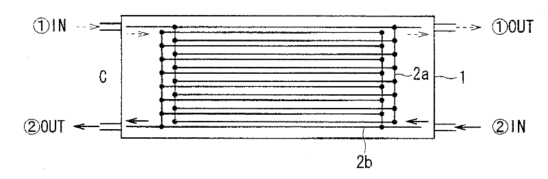
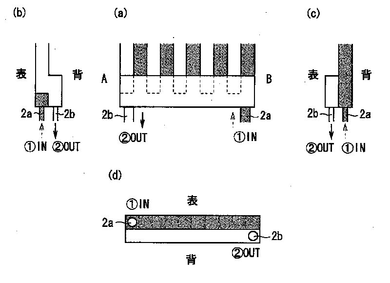
[0055] image 3 , Figure 4 It is a block diagram of the semiconductor wafer cooling apparatus of Embodiment 3. In the semiconductor wafer cooling device of this embodiment, a plurality of semiconductor wafers 10 are placed on the loading surface of the tray 1 (see figure 1 ). A pair of cooling ducts 2a, 2b are formed inside the tray 1, and the semiconductor wafer 10 is cooled by a cooling medium such as cooling water flowing in opposite directions through the cooling ducts 2a, 2b.
[0056] The cooling ducts 2a and 2b each have a structure in which a plurality of branch ducts are connected in parallel, and the branch ducts of the cooling duct 2a and the branch ducts of the cooling duct 2b are alternately arranged on a plane parallel to the mounting surface of the tray 1 .
[0057] Figure 4 (a) is the figure which looked at the cooling duct 2a, 2b from the back side of the tray 1 (the surface opposite to a mounting surface), Figure 4 (b) is from Figure 4 (a) View the c...
PUM
 Abstract
Description
Claims
Application Information
 - R&D
- Intellectual Property
- Life Sciences
- Materials
- Tech Scout
- Unparalleled Data Quality
- Higher Quality Content
- 60% Fewer Hallucinations
Browse by: Latest US Patents, China's latest patents, Technical Efficacy Thesaurus, Application Domain, Technology Topic, Popular Technical Reports.
© 2025 PatSnap. All rights reserved.Legal|Privacy policy|Modern Slavery Act Transparency Statement|Sitemap|About US| Contact US: help@patsnap.com