Semiconductor memory device and manufacturing method thereof

A manufacturing method and semiconductor technology, applied in semiconductor/solid-state device manufacturing, semiconductor devices, electric solid-state devices, etc., can solve the problems of poor compatibility of logic devices, poor anti-interference ability, weak gate-controlled diodes, etc., and achieve mask and The effect of reducing the number of processes and stabilizing the process

Active Publication Date: 2012-03-14
SUZHOU ORIENTAL SEMICONDUCTOR CO LTD
View PDF4 Cites 17 Cited by
  • Summary
  • Abstract
  • Description
  • Claims
  • Application Information

AI Technical Summary

Problems solved by technology

[0010] Although a semiconductor memory device using a recessed channel achieves a longer data retention time, it is less compatible with logic devices
At the same ...

Method used


Image

  • Semiconductor memory device and manufacturing method thereof
  • Semiconductor memory device and manufacturing method thereof
  • Semiconductor memory device and manufacturing method thereof

Examples


Embodiment Construction

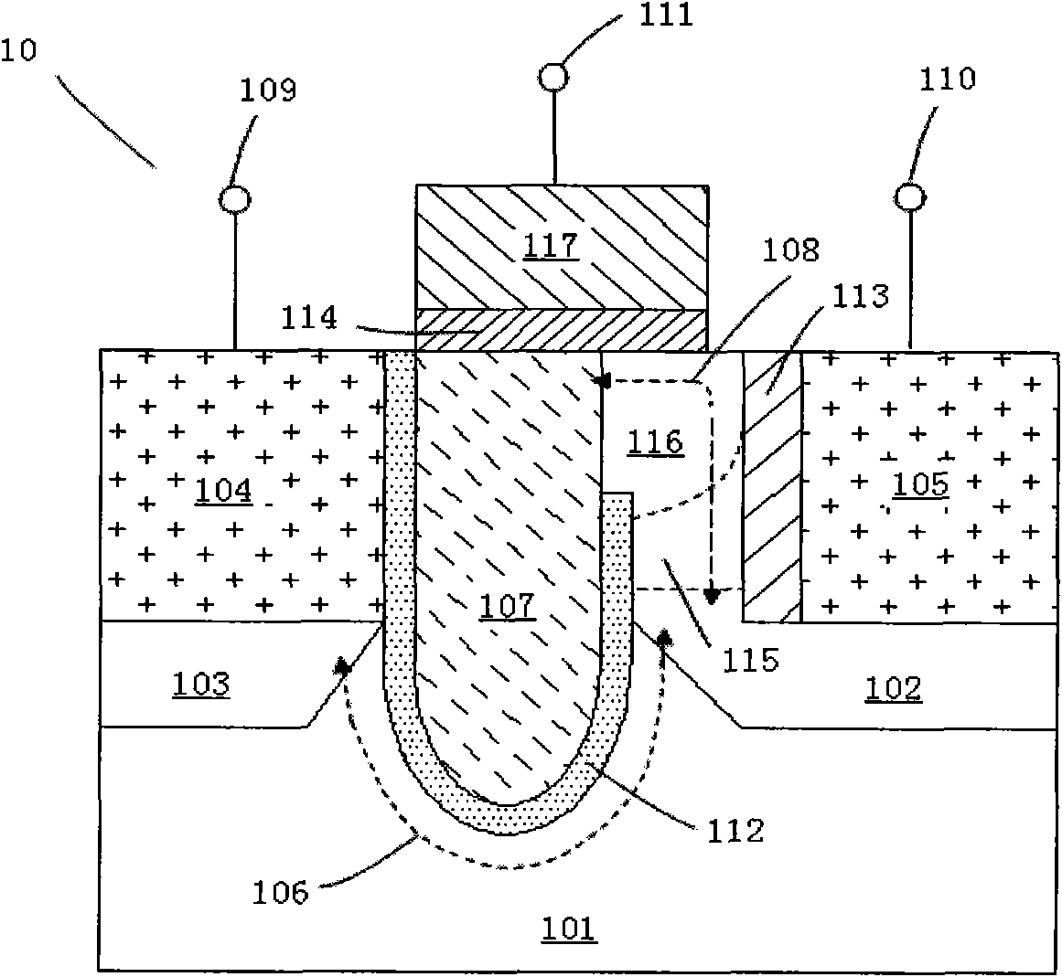
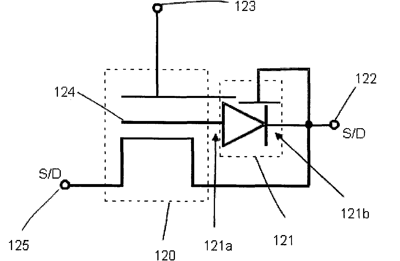
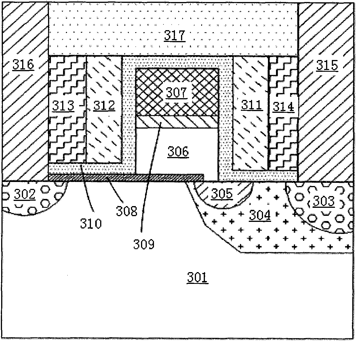
[0053] The present invention will be further described in detail below in conjunction with the accompanying drawings and specific embodiments. In the drawings, the thicknesses of layers and regions are exaggerated for convenience of illustration, and the shown sizes do not represent actual sizes. Although these figures do not completely reflect the actual size of the device, they still fully reflect the mutual positions between the regions and the constituent structures, especially the upper-lower and adjacent relationships between the constituent structures.

[0054] The referenced figures are schematic illustrations of idealized embodiments of the invention, and the illustrated embodiments of the invention should not be construed as limited to the particular shapes of regions illustrated in the figures but are to include resulting shapes, such as manufacturing-induced deviations. For example, the curves obtained by etching are usually curved or rounded, but in the embodiment...


PUM

PropertyMeasurementUnit
Thicknessaaaaaaaaaa
Thicknessaaaaaaaaaa

Abstract

The invention discloses a semiconductor memory device, which comprises at least one semiconductor substrate, a source electrode, a drain electrode, a floating gate area, two control gate electrodes and a gate control p-n junction diode. The gate control p-n junction diode is used for connecting the floating gate area and the substrate. In the semiconductor memory device, the floating gate area is used for storing information, and charging and discharging the floating gate area through the gate control p-n junction diode is realized. Furthermore, the invention also discloses a manufacturing method of the semiconductor memory device, a self-aligning process is adopted for manufacturing, and the process is simple and stable. Moreover, a planar channel structure is adopted, and the method is compatible with manufacturing of logic devices and flash memory devices.

Description

technical field [0001] The invention relates to a semiconductor memory device and a manufacturing method thereof, in particular to a planar channel type semiconductor memory device using two control gates and a manufacturing method thereof, belonging to the technical field of semiconductor memory. Background technique [0002] Semiconductor memories are widely used in various electronic products. Different application areas place different requirements on the structure, performance and density of semiconductor memories. For example, static random access memory (SRAM) has high random access speed and low integration density, while standard dynamic random access memory (DRAM) has high density and medium random access speed. [0003] Existing semiconductor random access memory units mainly include a single-transistor single-capacitor (1T-1C) DRAM unit, a 6-transistor (6-T) SRAM unit and a single-transistor floating body cell (FBC) memory unit. [0004] For a 1T-1C memory cell...

Claims


Application Information

Patent Timeline
IPC IPC(8): H01L27/10H01L29/10H01L29/423H01L21/8249
Inventor 刘磊王鹏飞刘伟
Owner SUZHOU ORIENTAL SEMICONDUCTOR CO LTD
Why Eureka
Try Eureka