Method for preparing semiconductor photoelectric device

A technology of optoelectronic devices and semiconductors, applied in the direction of semiconductor devices, electrical components, circuits, etc., can solve problems such as no mention of substrate requirements, and achieve a wide range of functions

Inactive Publication Date: 2012-03-14
王浩
View PDF6 Cites 36 Cited by
  • Summary
  • Abstract
  • Description
  • Claims
  • Application Information

AI Technical Summary

Problems solved by technology

Sun Yat-sen University Yang Guowei applied for a patent number of 200710027353 in 2007 for a heterogeneous p-n junction nanowire array and its preparation method and application. He invented a heterogeneous p-n junction nanowire array using pulsed laser deposition technology in a high temperature and high pressure environment. and its preparation method, no mention of substrate requirements
In 2002, Chen Xing's patent No. 02118371 was a nanowire light-emitting element and display device. In this invention, semiconductor materials were made into nano-single crystal wires or nano-single crystal columns, and the nanowires were grown on a transparent conductive substrate (or coated with a transparent conductive film. glass substrate) and made into a P, N interface structure, without mentioning the substrate requirements

Method used


Image

  • Method for preparing semiconductor photoelectric device
  • Method for preparing semiconductor photoelectric device
  • Method for preparing semiconductor photoelectric device

Examples


Embodiment 1

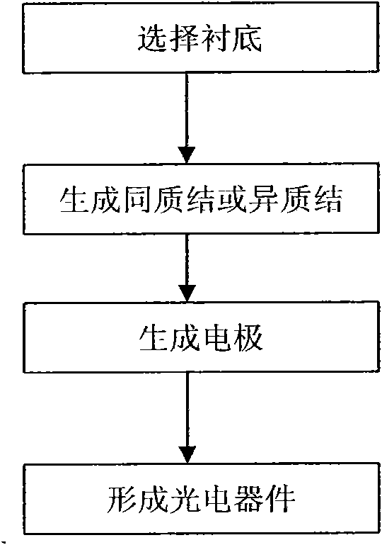
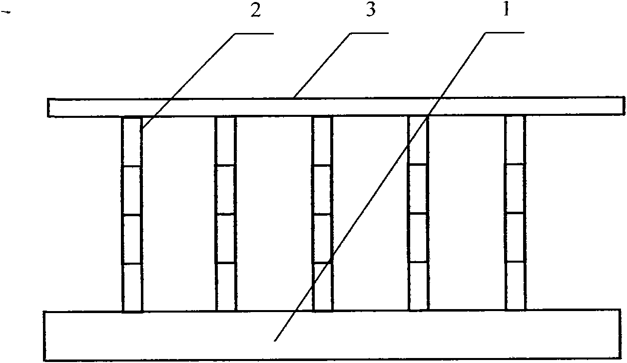
[0026] Such as figure 1 , figure 2 Shown, the preparation method of semiconductor optoelectronic device of the present invention, comprises the following steps:

[0027] First, select a Si with a semiconductor multilayer homojunction as the substrate 1; then, use epitaxy, crystallization, sputtering, evaporation, spin coating, bonding, welding, bonding, chemical corrosion or etching GaN / GaInN nanowire multilayer homojunction / heterostructure 2 is generated on the substrate 1. This structure has several extremely thin doped layers at the junction with the substrate, and finally a transparent metal film is formed on the structure. The top electrode 3 makes the substrate 1, the semiconductor homojunction or heterojunction 2 and the electrodes constitute the whole semiconductor device.

Embodiment 2

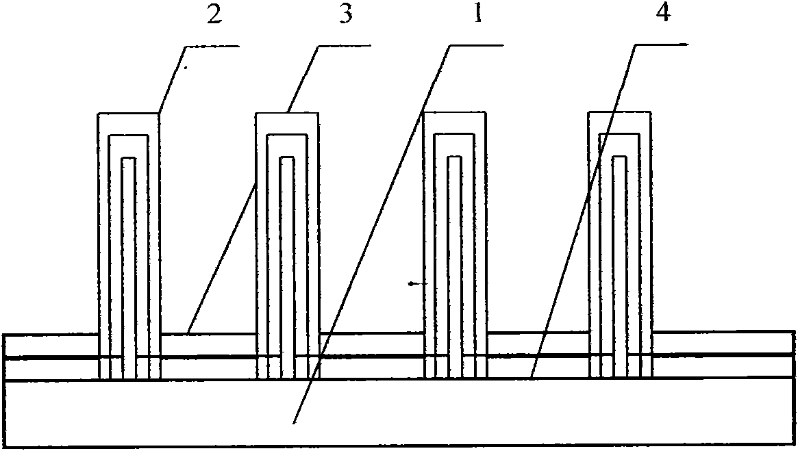
[0029] Such as figure 1 , image 3As shown, the preparation method of the semiconductor optoelectronic device of the present invention comprises the following steps: first, select a GaN(n) / GaN(p) / tunneling junction / GaInN(n) having a semiconductor multilayer homojunction / heterojunction / GaInN(p) as the substrate 1; then, use selective epitaxy or selective etching to generate a multi-layer GaAs / GaInP nanowire coaxial heterostructure 2, and make the outer layer of nanowires and the substrate The space is separated by a dielectric material film 4; finally, the electrode 3 of a transparent metal film is plated on the dielectric material film 4, so that the substrate 1, semiconductor homojunction or heterojunction 2 and the electrode 3 constitute the entire semiconductor device.

[0030] other embodiments

[0031] On the basis of Example 2, the substrate described in this example adopts a polycrystalline, amorphous, multilayer thin film or multilayer junction structure, and the th...


PUM


Abstract

The invention discloses a method for preparing a semiconductor photoelectric device, which comprises the following steps: 1) selecting a substrate; 2) preparing a semiconductor homojunction or heterojunction on the substrate by utilizing the processes of epitaxy, crystallizing, sputtering, evaporating, rotary coating, bonding, welding, linking, chemically corroding or etching; and 3) generating an electrode at the top end or bottom end of the semiconductor homojunction or heterojunction, thereby forming a whole semiconductor device by the substrate, the semiconductor homojunction or heterojunction and the electrode. According to the method provided by the invention, semiconductor junctions in various bandwidths can be provided, a wider working spectral region can be covered, the semiconductor junctions can be prepared on the substrates having different specific structures, and the advantages in preparation and performance characteristics of a planar film structure and a nanometer line are combined together, thereby realizing a semiconductor photoelectric device structure having a wider function.

Description

technical field [0001] The invention relates to a method for preparing a semiconductor photoelectric device, belonging to the field of semiconductor device preparation. Background technique [0002] Due to the breakthrough of semiconductor material preparation technology, especially with the breakthrough of nanometer-sized semiconductor crystal epitaxy preparation technology, the quality and performance of semiconductor materials have made major breakthroughs, making their applications in optoelectronic devices more and more. Patents on solar energy such as: the application number is 200780048752, the active area has a solar cell with a nanostructure with an energy well, and James C. Jin of Sandy Ord Company applied in 2007, which relates to a kind of solar cell with gradient energy Method and apparatus for a solar cell well. The active area of ​​the solar cell contains nanostructures. The nanostructure is formed from a material comprising a III-V compound semiconductor an...

Claims


Application Information

Patent Timeline
Patent Type & Authority Applications(China)
IPC IPC(8): H01L31/18H01L33/00
CPCY02P70/50
Inventor 王浩
Owner 王浩
Why Eureka
Try Eureka