

Solid-state imaging device, manufacturing method thereof, and electronic apparatus
A technology of a solid-state imaging device and a manufacturing method, which is applied in the direction of semiconductor/solid-state device manufacturing, electric solid-state device, and final product manufacturing, etc., can solve problems related to difficult mass production, undesired reliability of wiring layers, adhesion and durability. and other problems, to achieve the effect of improving light absorption efficiency, improving sensitivity, and improving charge mobility.
Inactive Publication Date: 2012-03-21
SONY CORP
View PDF7 Cites 6 Cited by
- Summary
- Abstract
- Description
- Claims
- Application Information
AI Technical Summary
Problems solved by technology
Also, the formation process of the photoelectric conversion portion includes many heat treatment steps, which is not desirable for the reliability of the wiring layer (occurrence of cracks, etc.)
Also, in the current process technology, when the film is produced under atmospheric pressure by roll-to-roll processing, there are problems related to the adhesion and durability of the film, and it is not easy to mass-produce
Method used
View moreImage
Smart ImageViewing Examples

Examples
no. 1 approach
[0041] 3. First Embodiment (Arrangement Example of Solid-State Imaging Device and Example of Manufacturing Method thereof)
[0042] 4. Second Embodiment (Arrangement Example of Solid-State Imaging Device and Example of Manufacturing Method thereof)
no. 3 approach
[0043] 5. Third Embodiment (Arrangement Example of Solid-State Imaging Device and Example of Manufacturing Method thereof)
no. 4 approach
[0044] 6. Fourth Embodiment (Arrangement Example of Solid-State Imaging Device and Example of Manufacturing Method thereof)
Login to View More PUM
 Abstract
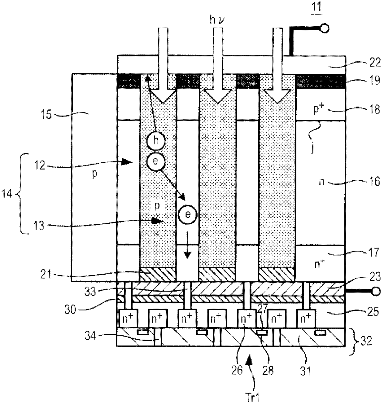
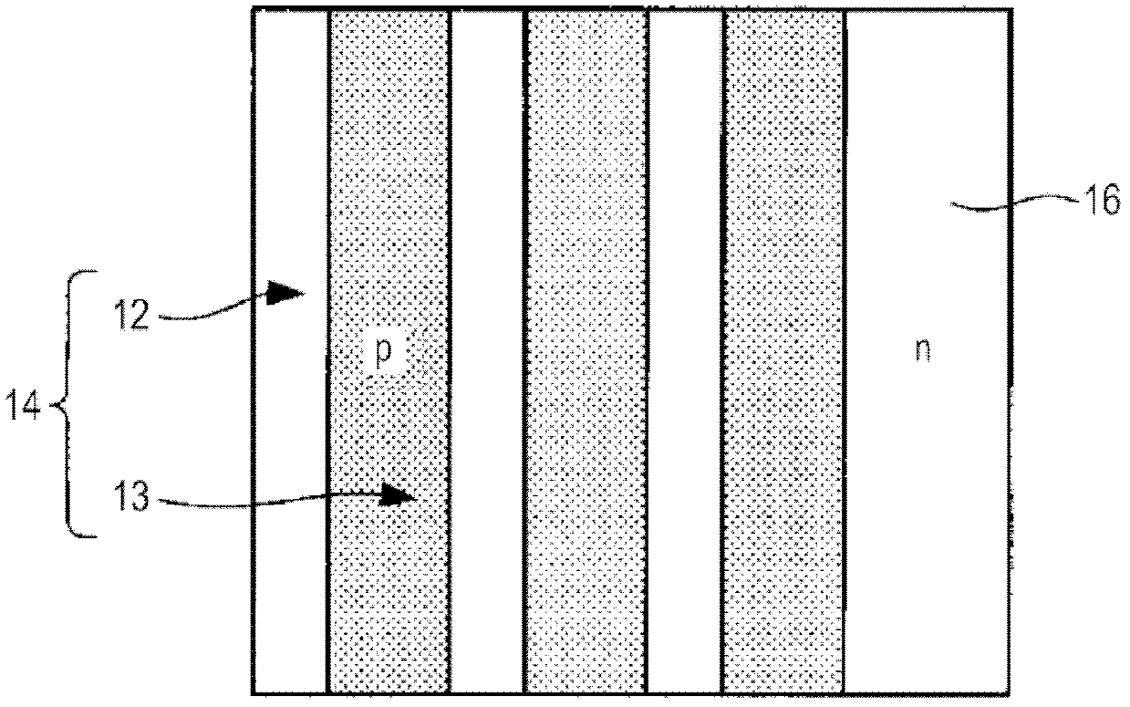
The invention provides a solid-state imaging device, a manufacturing method thereof, and an electronic apparatus comprising the solid-state imaging device. The solid-state imaging device includes: pixels each including a hybrid photoelectric conversion portion and pixel transistors, wherein the hybrid photoelectric conversion portion includes a semiconductor layer having a p-n junction, a plurality of columnar or cylindrical hollow-shaped organic material layers disposed in the semiconductor layer, and a pair of electrodes disposed above and below the semiconductor layer and the organic material layers, wherein charges generated in the organic material layers through photoelectric conversion move inside the semiconductor layer so as to be guided to a charge accumulation region, and wherein the solid-state imaging device is configured as a back-illuminated type in which light is incident from a surface opposite to the surface on which the pixel transistors are formed. The solid-state imaging device in the invention improves sensitivity and can realize high-speed and stable drive.
Description
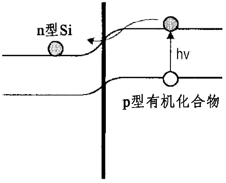
[0001] Cross References to Related Applications [0002] This application contains subject matter related to and claims priority from Japanese Patent Application JP2010-189284 filed in the Japan Patent Office on Aug. 26, 2010, the entire content of which is hereby incorporated by reference. technical field [0003] The present invention relates to a solid-state imaging device, a manufacturing method thereof, and electronic equipment such as a camera having the solid-state imaging device. Background technique [0004] Solid-state imaging devices (image sensors) are classified into two types: a front-illuminated type and a back-illuminated type. Also, there is known a solid-state imaging device in which a photoelectric conversion portion is formed of a silicon-based photodiode or an organic material layer. [0005] In a solid-state imaging device having a silicon-based photodiode, the photodiode is formed of a crystalline silicon layer implanted with impurities, and serves to...
Claims
Login to View More Application Information
Patent Timeline
 Patent Type & AuthorityApplications(China)
IPC IPC(8): H01L27/30H04N5/225H01L51/48H04N25/00
CPCY02E10/549H04N5/335H01L27/1464H01L27/307Y02P70/50H10K39/32H01L27/146H04N25/00
Inventor久保井信行
OwnerSONY CORP