Photovoltaic cell

A photovoltaic cell and battery technology, applied in photovoltaic power generation, circuits, electrical components, etc., can solve problems such as difficulty in accurately controlling the thickness of the n-type doped layer, improve open circuit voltage and overall efficiency, reduce doping concentration, and improve compounding. effect of life

Active Publication Date: 2012-03-21
IQE SILICON COMPOUNDS
View PDF6 Cites 8 Cited by
  • Summary
  • Abstract
  • Description
  • Claims
  • Application Information

AI Technical Summary

Problems solved by technology

However, it is still difficult to precisely control the thickness of the n-type doped layer using the described technique, the boundary between the n-type doped region and the p-type doped region is diffuse in nature, and the concentration of n-type doping must be high to offset Bulk p-type doping of the substrate

Method used


Image

  • Photovoltaic cell
  • Photovoltaic cell
  • Photovoltaic cell

Examples


Embodiment Construction

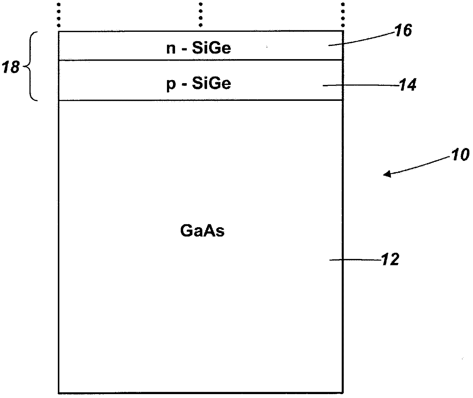
[0033] see Figure 1A , which schematically shows the photovoltaic cell structure 10 according to the first embodiment of the present invention. The structure 10 includes a GaAs substrate 12 . On said GaAs substrate there are two continuous first layers 14 , 16 of SiGe material epitaxially grown on the GaAs substrate and monolithic therewith, these layers together forming a first germanium-based photovoltaic junction 18 . The silicon content of the first layer of SiGe is chosen to substantially lattice match the GaAs substrate. For this reason, Si x Ge 1-x The silicon fraction x may be 0-0.04, more preferably 0.01-0.03, still more preferably 0.016-0.02. To form a practical photovoltaic junction, the lower SiGe layer can typically be doped p-type to a concentration of about 5×10 16 cm -3 ~5×10 19 cm -3 , and the thickness is about 1 μm to 2 μm. The upper SiGe layer can typically be n-type doped to a concentration of about 1 x 10 17 cm -3 , and the thickness is about 0...


PUM


Abstract

There is disclosed a photovoltaic cell, such as a solar cell, incorporating one or more epitaxially grown layers of SiGe or another germanium material, substantially lattice matched to GaAs. A GaAs substrate used for growing the layers may be removed by a method which includes using a boundary between said GaAs and the germanium material as an etch stop.

Description

technical field [0001] The present invention relates to photovoltaic cells, in particular (but not exclusively) to multi-junction solar cells in which the lower photovoltaic junction for absorbing the long wave portion of the solar spectrum is germanium based. Background technique [0002] Photovoltaic cells convert light energy, such as sunlight, into useful electrical energy. Typically, electron-hole pairs are formed by the absorption of photons in semiconductor materials adjacent to p-n junctions that act to separate charge carriers, which are then transported into electrical circuits through metal contacts on the battery device. This absorption process occurs only when the photon energy is higher than the bandgap of the local semiconductor material, so low-bandgap materials tend to absorb more photons. The excess energy of a photon above the bandgap energy is lost as heat within the semiconductor lattice. If the p-n junction is made of a material with a high band gap, ...

Claims


Application Information

Patent Timeline
Patent Type & Authority Applications(China)
IPC IPC(8): H01L31/0693H01L31/0687H01L31/18
CPCH01L31/0687H01L31/18H01L31/028Y02E10/544Y02E10/547H01L31/042H01L31/068H01L31/0682H01L31/0684H01L31/1808H01L31/1812
Inventor R·C·哈珀
Owner IQE SILICON COMPOUNDS
Why Eureka
Try Eureka