U-shaped electromagnetic band gap circuit board with low-frequency simultaneous switching noise inhibiting function

An electromagnetic bandgap and switching noise technology, applied in printed circuit components and other directions, can solve the problems of inability to effectively suppress low-frequency simultaneous switching noise, reduce equipment reliability, malfunction of electronic devices, etc., to reduce the difficulty of etching, The effect of improving production efficiency and reducing the interference of high-frequency signals

Inactive Publication Date: 2012-03-28
XIDIAN UNIV
View PDF9 Cites 5 Cited by
  • Summary
  • Abstract
  • Description
  • Claims
  • Application Information

AI Technical Summary

Problems solved by technology

However, the cut-off frequency of these new EBG structure band gaps is higher than 600MHz, which cannot effectively suppress the simultaneous switching noise SSN in the low frequency band, and this noise will cause serious interference to the normal transmission of high frequency signals, causing electronic devices to malfunction. Reduce equipment reliability and increase maintenance costs

Method used


Image

  • U-shaped electromagnetic band gap circuit board with low-frequency simultaneous switching noise inhibiting function
  • U-shaped electromagnetic band gap circuit board with low-frequency simultaneous switching noise inhibiting function
  • U-shaped electromagnetic band gap circuit board with low-frequency simultaneous switching noise inhibiting function

Examples


Embodiment Construction

[0018] The present invention will be described in further detail below with reference to the accompanying drawings.

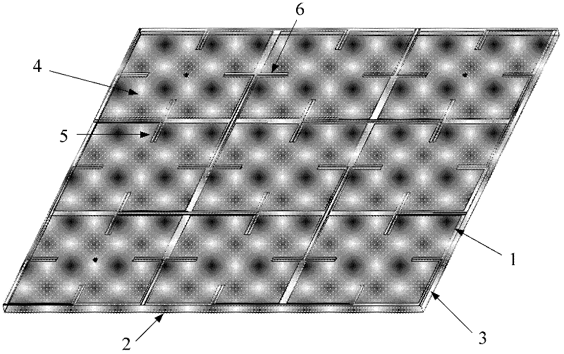
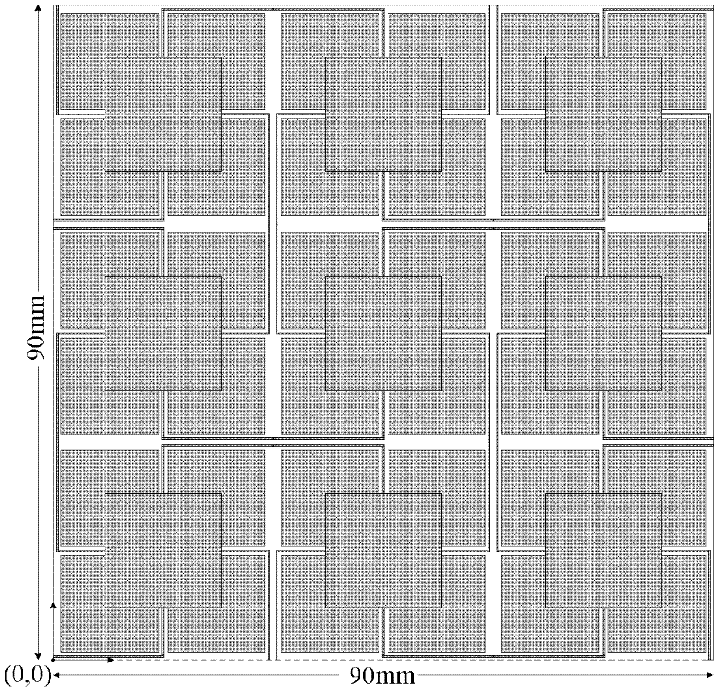
[0019] refer to figure 1 with figure 2 , The 3×3U electromagnetic bandgap circuit board of the present invention includes: an electromagnetic bandgap layer 1 , a ground layer 2 and a dielectric layer 3 . Among them, the electromagnetic bandgap layer 1 and the formation 2 are made of copper, and the relative permittivity is 1; the dielectric layer 3 is made of FR4 material with a thickness of 0.4mm, and the relative permittivity is 4.4; the electromagnetic bandgap layer consists of 9 electromagnetic bandgap Unit 4 is connected to form. in:

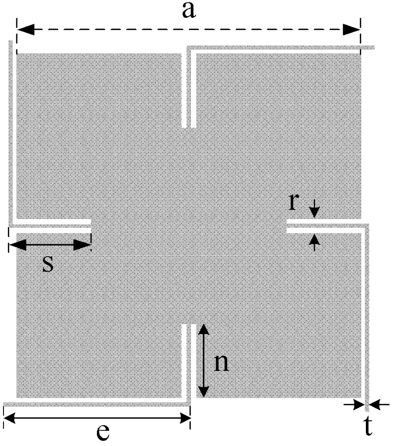
[0020] For the electromagnetic bandgap unit located on the left side of the first row, the first segment of the L-shaped connecting line in the left rectangular slot is rotated 90 degrees and folded upwards to the second straight line, and the L-shaped connecting line in the right rectangular slot is first The first sec...


PUM


Abstract

The invention discloses a U-shaped electromagnetic band gap circuit board with a low-frequency simultaneous switching noise inhibiting function, which mainly solves the problem that the existing electromagnetic band gap circuit board has limited capacity on inhibiting low-frequency simultaneous switching noise with the frequency lower than 1GHz. The electromagnetic band gap circuit board consistsof an electromagnetic band gap layer (1), a stratum (2) and a dielectric layer (3), wherein the electromagnetic band gap layer (1) is formed by connecting n electromagnetic band gap units (4) and thenumber n is determined according to actual engineering needs. The middle position of each edge of the electromagnetic band gap units (4) is provided with a rectangular slot (5), an L-shaped connecting line (6) is led out from the middle position of the rectangular groove from inside to outside, and every two electromagnetic band gap units (4) are symmetrically connected through one L-shaped connecting line to form a U-shaped bridging line, so the electromagnetic band gap units (4) are connected to form the electromagnetic band gap layer (1). The U-shaped electromagnetic band gap circuit boarddisclosed by the invention has stronger capacity in inhibiting the low frequency range simultaneous switching noise, can reduce the interference of the noise on signal transmission and the false operation of electronic devices, and can be used in high frequency electronic circuits of microwaves, antennae and communication.

Description

technical field [0001] The invention belongs to the technical field of electronic devices, and relates to a novel circuit board with a coplanar electromagnetic bandgap structure, which has a stronger ability to suppress simultaneous switching noise in a low-frequency band lower than 1 GHz, and can be used for microwaves, antennas, and communications, etc. High frequency electronic circuits. Background technique [0002] As the clock frequency of modern digital circuits continues to increase, a signal integrity problem called "simultaneous switching noise SSN" has become a bottleneck restricting the design and manufacture of high-speed circuits. Therefore, designers focus on how to suppress and eliminate SSN. The traditional solutions mainly include: setting a discrete decoupling capacitor between the power layer and the ground layer to form a low-impedance return path, but when the noise frequency is higher than 600MHz, the effect of the decoupling capacitor will be greatly...

Claims


Application Information

Patent Timeline
Patent Type & Authority Applications(China)
IPC IPC(8): H05K1/02
Inventor 叶强史凌峰张科来新泉甑立冬
Owner XIDIAN UNIV
Why Eureka
Try Eureka