Electrically conductive ink, and laminate having electrically conductive pattern attached thereto and process for production thereof
A technology of conductive ink and conductive pattern, which is applied in the manufacture of cables/conductors, conductive materials dispersed in non-conductive inorganic materials, conductive layers on insulating carriers, etc., can solve the problems of complicated manufacturing steps, weakening of physical impact, and Many problems, to achieve the effect of excellent resistance value stability
- Summary
- Abstract
- Description
- Claims
- Application Information
AI Technical Summary
Problems solved by technology
Method used
Image
Examples
Embodiment 1
[0255] Example 1
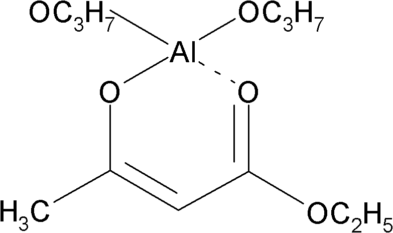
[0256] Mixing with a disperser: the binder (1) solution containing 40 parts by weight of epoxy resin: 100 parts by weight; the metal chelate compound A containing 0.81 parts by weight of ethyl acetoacetate aluminum diisopropionate: 0.9 parts by weight Parts, silver powder A: 330 parts by weight, diethylene glycol monoethyl ether acetate: 40 parts by weight, dispersed with three rolls, and prepared conductive ink.
[0257] The obtained conductive ink had a solid content of about 79% by weight, in a total of 370 parts by weight of the epoxy resin and silver powder, about 89% by weight of the silver powder, and 11% by weight of the epoxy resin.
[0258] Next, using a rheometer (rheometer) "AR-G2" manufactured by TA Instruments Co., Ltd., at a temperature of 25°C, fixed at a frequency of 1 Hz, and under a vibration stress range of 1.0 to 100,000 Pa, dynamics such as the storage elastic coefficient G' were measured. Regarding the viscoelastic properties, the st...
Embodiment 2 to 9、 comparative example 1 to 9
[0259] Examples 2 to 9, Comparative Examples 1 to 9
[0260] Silver powder, binder resin solution, metal chelate, hardener, and solvent were mixed in a disperser at the mixing ratio shown in Tables 1 and 2, and then dispersed with three rolls to prepare conductive ink in the same manner as in Example 1. The properties of the obtained conductive ink were measured by the following methods.
[0261] [Preparation of test piece]
[0262] On a corona-treated polyethylene terephthalate film (hereinafter referred to as PET) with a thickness of 75 μm, the conductive inks of Examples 1 to 12 and Comparative Examples 1 to 9 are screen-printed into a pattern of 15 mm × 30 mm shape, and dried in a 150°C oven for 30 minutes to obtain a conductive printed matter with a film thickness of 8 to 10 μm.
[0263]
[0264] The film thickness of the said printed matter was measured using the MH-15M type measuring device by Sendai Nikon company.
[0265]
[0266] The said printed matter surfa...
PUM
| Property | Measurement | Unit |
|---|---|---|
| specific surface area | aaaaa | aaaaa |
| hydroxyl value | aaaaa | aaaaa |
| density | aaaaa | aaaaa |
Abstract
Description
Claims
Application Information


