Array substrate, fabricating method for same and liquid crystal display panel

An array substrate and display area technology, which is applied in semiconductor/solid-state device manufacturing, instruments, semiconductor devices, etc., can solve the problem of the size limitation of 320 in the display area and cannot be further enlarged, and achieves improved utilization, area saving, and crosstalk reduction. Effect

Active Publication Date: 2015-05-20
SHANGHAI TIANMA MICRO ELECTRONICS CO LTD
View PDF5 Cites 0 Cited by
  • Summary
  • Abstract
  • Description
  • Claims
  • Application Information

AI Technical Summary

Problems solved by technology

This causes the size of the display area 320 to be limited and cannot be further enlarged

Method used


Image

  • Array substrate, fabricating method for same and liquid crystal display panel
  • Array substrate, fabricating method for same and liquid crystal display panel
  • Array substrate, fabricating method for same and liquid crystal display panel

Examples


no. 1 example

[0063] refer to Figure 5 , is a schematic top view structure diagram of the array substrate according to the first embodiment of the present invention.

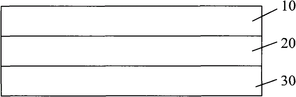
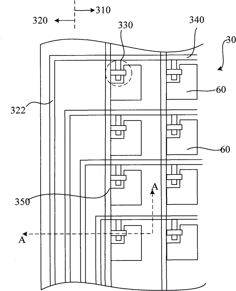
[0064] The array substrate is divided into a display area and a frame area surrounding the display area. To simplify the illustration, Figure 5 Only a schematic top view of a part of the display area is shown in . The display area includes: a glass substrate; multiple scanning lines on the glass substrate: scanning line 101, scanning line 103, scanning line 105, etc., multiple data lines: data line 102, data line 104, data line 106, etc. , each scan line is orthogonal to the data line and is insulated from each other. The data line and the scan line are made of different layers of metal. The data line is located above the scan line. The two divide the display area into a plurality of pixel areas arranged in an array. Each pixel area includes a thin film transistor 110 and a pixel electrode 120 .

[0065] Figure 5 The a...

no. 2 example

[0090] In the above-mentioned embodiments, the scanning connection line and the scanning line are electrically connected through vias using other conductive layers, and processes such as alignment, etching, and conductive layer deposition for forming the via holes on the scanning connection line and the scanning line are required. . As another optional embodiment, the scanning connection line and the scanning line may also be directly electrically connected without using other conductive layers, thereby simplifying the structure of the array substrate and improving connection reliability.

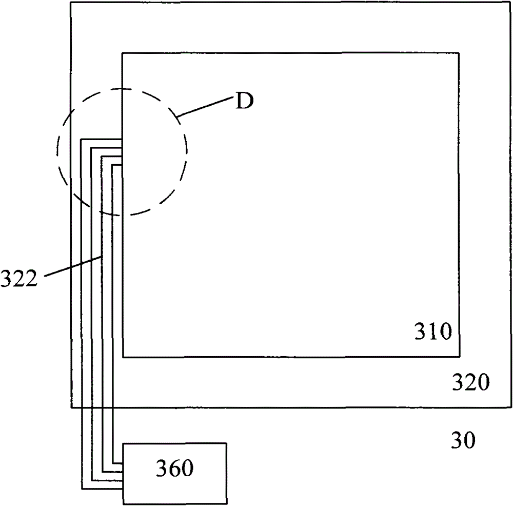
[0091] Specifically, refer to Figure 20 As shown in FIG. 2 , it is a schematic top view structure diagram of the array substrate according to the second embodiment of the present invention. Will Figure 19 and Figure 5 It can be seen from the comparison that the difference between this embodiment and the first embodiment is that the connection structure between the scanning connection ...


PUM


Abstract

The invention provides an array substrate, a fabricating method for the same and a liquid crystal display panel. The array substrate comprises a display area and a frame area enclosing the display area, and the display area comprises a plurality of data lines and a plurality of scanning lines, a plurality of pixel areas in array arrangement and a plurality of scanning connection lines, wherein the data lines and the scanning lines are orthogonal and insulated to one another and divide the display area into the pixel areas, each pixel area comprises a pixel electrode and a thin film transistor, the scanning connection lines are parallel to the data lines and used for electrically connecting the corresponding scanning lines with external driving chips. The scanning connection lines are arranged in the display area, and the scanning connection lines are used for transmitting signals by scanning a drive circuit to the corresponding scanning lines, so that the area of the scanning connection lines in a frame area is economized, and the utilization ratio of the substrate is improved.

Description

technical field [0001] The invention relates to a liquid crystal panel, in particular to an array substrate with a narrow frame design for reducing the frame width of the liquid crystal display panel to increase the display range, a manufacturing method thereof, and a liquid crystal display panel. Background technique [0002] Flat-panel displays are currently the most popular displays, among which liquid crystal displays are widely used in electronic products such as computer screens, mobile phones, personal digital assistants, and flat-screen TVs because of their thin and light appearance, power saving, and no radiation. [0003] Please refer to figure 1 , for an existing liquid crystal display panel. It includes a color filter substrate 10 and an array substrate 30 opposite to the color filter substrate 10 , and the liquid crystal layer 20 is sandwiched between the color filter substrate 10 and the array substrate 30 . The inner side of the array substrate 30 relative t...

Claims


Application Information

Patent Timeline
Patent Type & Authority Patents(China)
IPC IPC(8): H01L27/12G02F1/1362G02F1/1368G02F1/1333H01L21/77
Inventor 赵剑李治福刘金娥王超周兴雨
Owner SHANGHAI TIANMA MICRO ELECTRONICS CO LTD
Why Eureka
Try Eureka