
Wafer level image sensor packaging structure and manufacturing method thereof

The technology of an image sensor and manufacturing method, which is applied in the direction of radiation control devices, etc., can solve the problems of side light leakage, glare, poor image sensing quality, etc., and achieve the reduction of the height of the structure structure, the simplicity of the manufacturing process, and the reduction of the structure size Effect

Active Publication Date: 2012-04-04
KINGPAK TECH INC
View PDF6 Cites 11 Cited by
  • Summary
  • Abstract
  • Description
  • Claims
  • Application Information

AI Technical Summary

Problems solved by technology

Among them, the traditional COB packaging method needs to stick the image sensor chip on the substrate, use metal wires to electrically connect the substrate and the image sensor chip, and then package the image sensor chip through packaging technology, so the packaged image sensor structure The structure is large in size and has a certain height
The traditional chip-scale packaging method is more suitable for low-pixel image sensor chips. In the application field of higher pixels, the cost is not competitive, and when it is matched with the lens module due to the original glass structure, resulting in The height of the image sensor module is increased, and the image sensing quality is also worse than that of the COB package
In addition, the traditional chip-scale packaging method has the problem of side light leakage in the structure. Therefore, it is necessary to add a light shield or coat a light-shielding layer on the side of the structure in the image sensor module assembly process to avoid image sensing. Reduced quality or cause problems such as glare (Flare)
[0005] It can be seen that the above-mentioned existing wafer-level image sensor construction structure and its manufacturing method obviously still have inconveniences and defects in product structure, manufacturing method and use, and need to be further improved urgently.
In order to solve the above-mentioned problems, the relevant manufacturers have tried their best to find a solution, but no suitable design has been developed for a long time, and there is no suitable structure and method for general products and methods to solve the above-mentioned problems. This is obviously a problem that relevant industry players are eager to solve

Method used


Image

  • Wafer level image sensor packaging structure and manufacturing method thereof
  • Wafer level image sensor packaging structure and manufacturing method thereof
  • Wafer level image sensor packaging structure and manufacturing method thereof

Examples


Embodiment Construction

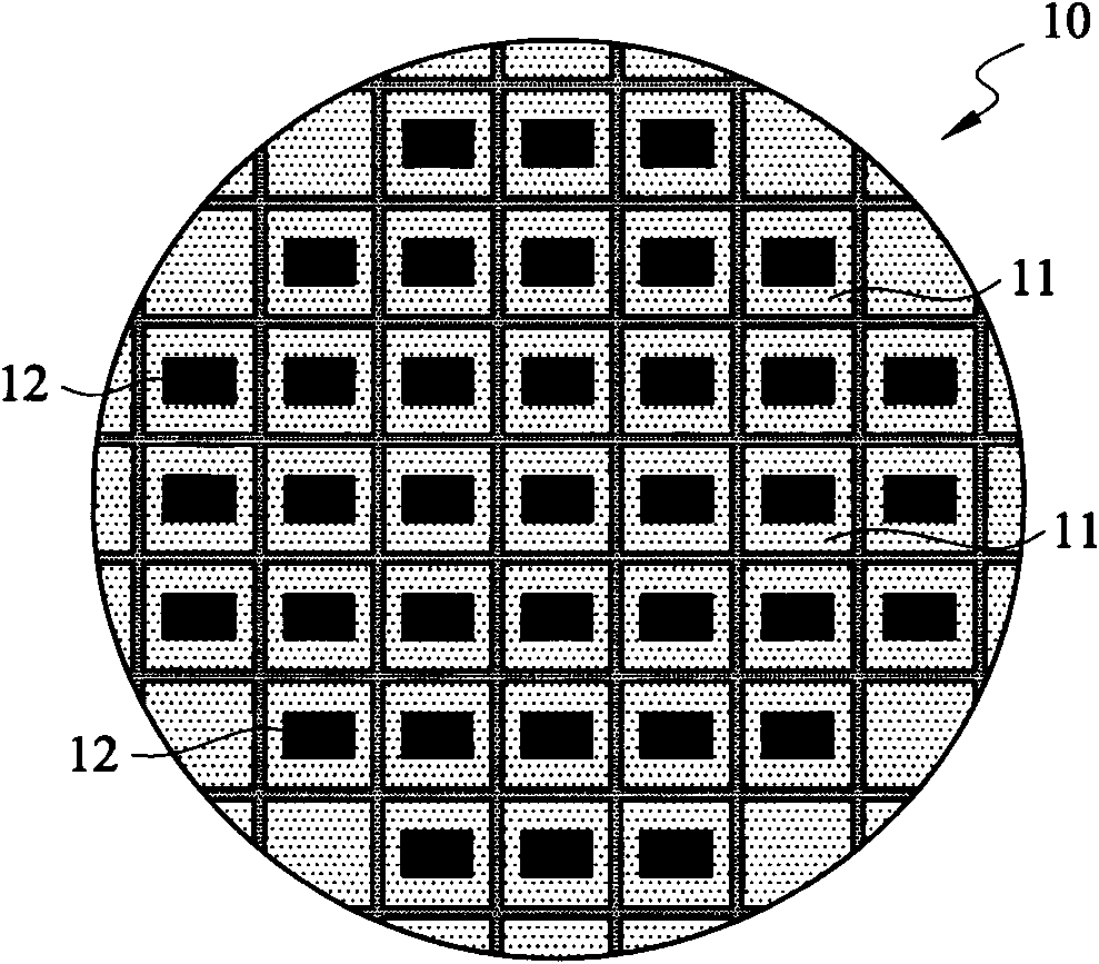
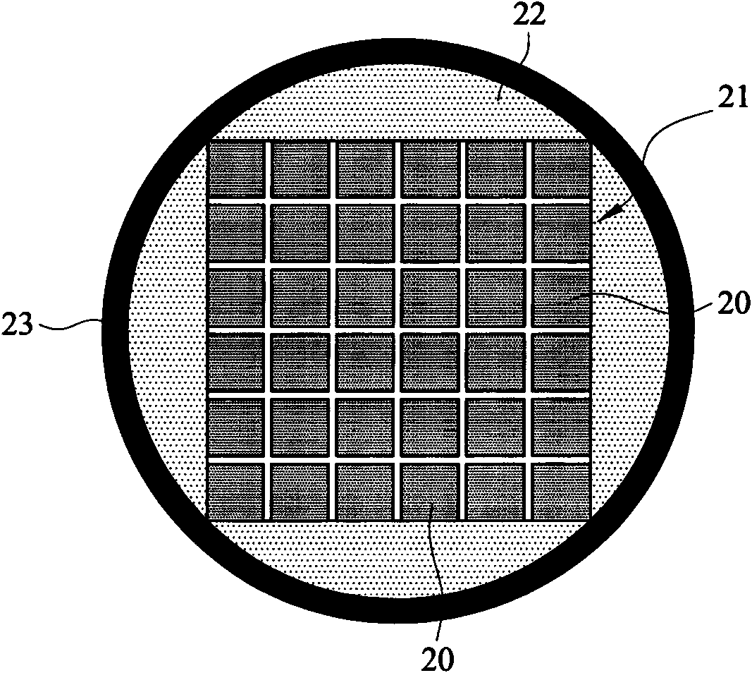
[0067] In order to further explain the technical means and effects of the present invention to achieve the intended purpose of the invention, the wafer-level image sensor assembly structure and its manufacturing method proposed according to the present invention will be described below in conjunction with the accompanying drawings and preferred embodiments. Specific embodiments, structures, methods, steps, features and effects thereof are described in detail below.

[0068] The aforementioned and other technical contents, features and effects of the present invention will be clearly presented in the following detailed description of preferred embodiments with reference to the drawings. Through the description of the specific implementation mode, a more in-depth and specific understanding of the technical means and effects adopted by the present invention to achieve the intended purpose can be obtained. However, the accompanying drawings are only for reference and description, a...


PUM


Abstract

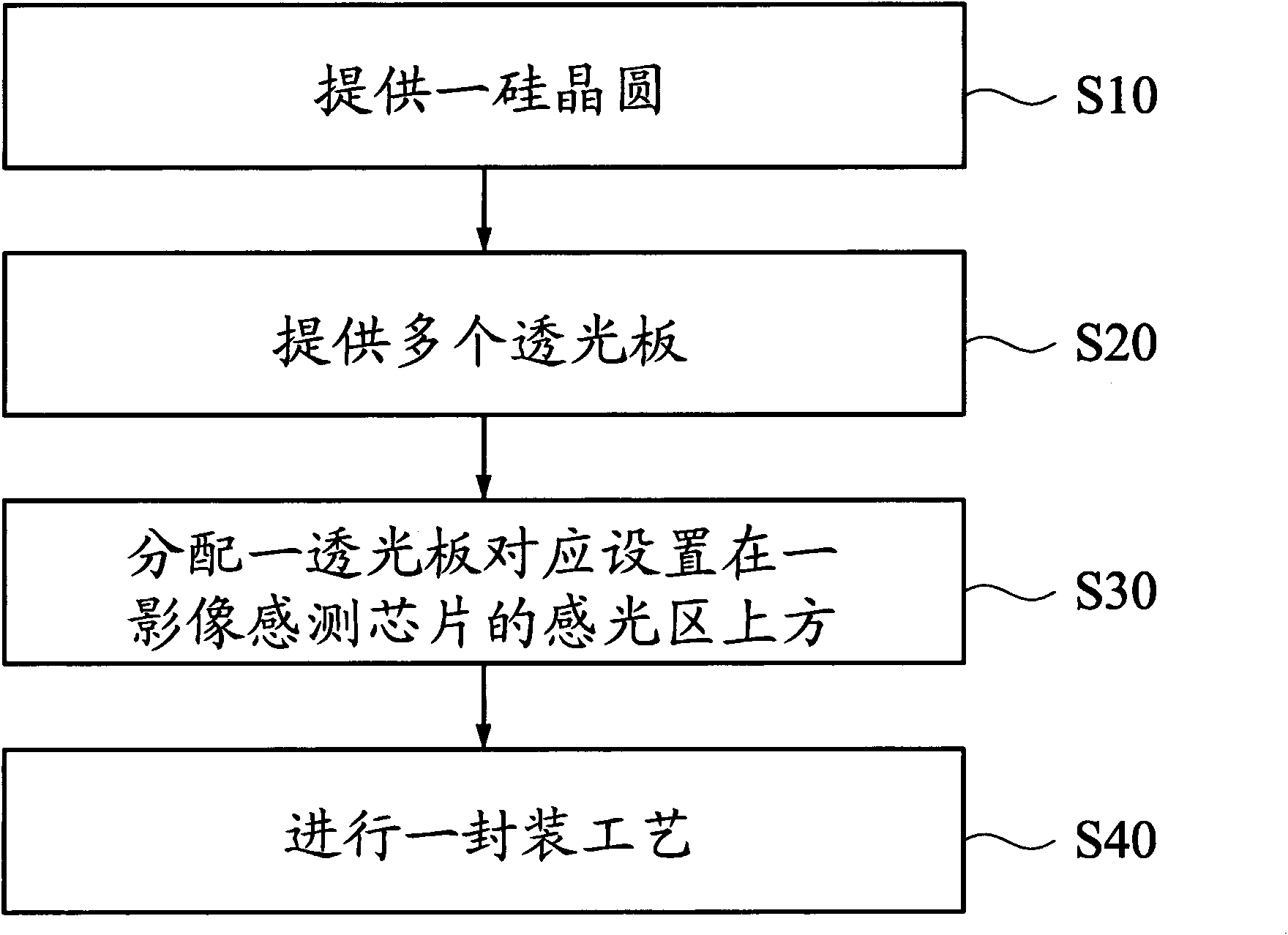
The invention relates to a wafer level image sensor packaging structure and a manufacturing method of the wafer level image sensor packaging structure, wherein the manufacturing method comprises the following steps of: providing a silicon wafer with an image sensor chip; providing a plurality of transparent boards; correspondingly arranging the distributed transparent boards above a photosensitive area of the image sensor chip; and packaging. The manufacturing method has the advantages of simplified manufacturing process, low manufacturing cost and high product yield; and as a plastic packaging material is arranged on the first surface of the image sensor chip and is coated on the peripheries of the transparent boards, the problem of side light leakage generated in a traditional chip size package (CSP) manner can be solved, and the image sensing efficiency of the wafer level image sensor packaging structure is further improved.

Description

technical field [0001] The present invention relates to a wafer-level image sensor assembly structure and a manufacturing method thereof, in particular to a wafer-level image sensor assembly structure applicable to batch-manufacturable image sensor assembly structures and its method of manufacture. Background technique [0002] In recent years, with the popularization of digital imaging products around the world, coupled with the hot sales of various digital imaging products such as camera phones, digital cameras, and digital video cameras, the market for digital imaging sensors has become very optimistic. [0003] Among them, the image sensor can be divided into charge-coupled device (Charge-coupled Device, CCD) and complementary metal-oxide-semiconductor (Complementary Metal-Oxide-Semiconductor, CMOS) according to its manufacturing process. , The image quality is good, but the cost will increase due to its special production technology. On the contrary, complementary met...

Claims


Application Information

Patent Timeline
IPC IPC(8): H01L27/146H01L27/148
Inventor 杜修文陈翰星辛宗宪陈明辉
Owner KINGPAK TECH INC
Learn More