Insulation treatment method for film solar cell
A solar cell, insulation treatment technology, applied in circuits, electrical components, sustainable manufacturing/processing, etc., can solve the problems of high operating costs, sand consumption, low equipment utilization rate, etc., to save input costs and operating costs , the effect of clean process and simple process
- Summary
- Abstract
- Description
- Claims
- Application Information
AI Technical Summary
Problems solved by technology
Method used
Image

Examples
Embodiment 1
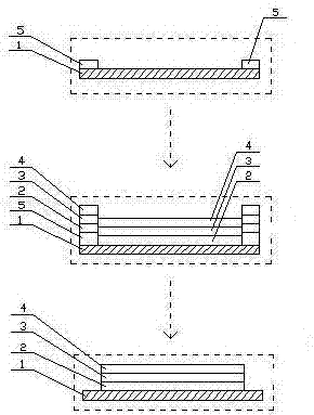
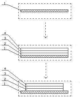
[0028] A kind of thin-film solar cell insulation treatment method, such as figure 1 As shown in the silicon-based thin-film solar cell, the coating includes a front electrode 2, an absorber layer 3, and a back electrode 4. The specific process is as follows:
[0029] Paste insulating tape 5 on the area around the surface of the glass 1 to be treated that needs to be cleared. Before deposition, the electrode 2 forms a conductive glass. After the conductive glass passes through laser and cleaning processes, it enters the coating equipment for the deposition of the absorbing layer 3. After laser etching , to form a film on the back electrode 4, and then after the third laser process, finally tear off the insulating tape, remove all the film layers on the edge of the thin film solar cell at one time, including the front electrode 2, the absorption layer 3 and the back electrode 4, and clean Finally, the insulation treatment of the battery is completed.
[0030] The insulating tap...
Embodiment 2
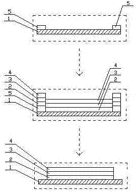
[0033] A thin-film solar cell insulation treatment method, the silicon-based thin-film solar cell, the coating includes a front electrode, an absorption layer, and a back electrode, and the specific process is as follows:
[0034] Paste insulating tape on the area around the surface of the glass to be treated that needs to be cleared. After depositing the front electrode to form conductive glass, tear off the insulating tape and remove the front electrode in this area; after the conductive glass has undergone laser and cleaning processes, paste it on the same area above A layer of insulating tape enters the coating equipment to deposit the absorbing layer. After laser etching, the back electrode is formed into a film. After the third laser process, the insulating tape is finally torn off to remove the absorbing layer on the edge of the thin film solar cell. And the back electrode, after cleaning, the insulation treatment of the battery is completed.
[0035] The insulating tap...
PUM
 Abstract
Description
Claims
Application Information
 - Generate Ideas
- Intellectual Property
- Life Sciences
- Materials
- Tech Scout
- Unparalleled Data Quality
- Higher Quality Content
- 60% Fewer Hallucinations
Browse by: Latest US Patents, China's latest patents, Technical Efficacy Thesaurus, Application Domain, Technology Topic, Popular Technical Reports.
© 2025 PatSnap. All rights reserved.Legal|Privacy policy|Modern Slavery Act Transparency Statement|Sitemap|About US| Contact US: help@patsnap.com