Semiconductor memory device and manufacturing method of the same

A technology of memory elements and semiconductors, applied in semiconductor devices, static memory, electric solid state devices, etc., can solve the problems of reducing tunneling magnetoresistance and achieve the effect of reducing write current

Active Publication Date: 2012-04-11
TAIWAN SEMICON MFG CO LTD
View PDF3 Cites 1 Cited by
  • Summary
  • Abstract
  • Description
  • Claims
  • Application Information

AI Technical Summary

Problems solved by technology

Some existing methods can reduce the write current, but also reduce the thermal stability of tunnel magnetoresistance (TMR) and spin torque transfer magnetic random access memory (STT-MRAM) devices

Method used


Image

  • Semiconductor memory device and manufacturing method of the same
  • Semiconductor memory device and manufacturing method of the same
  • Semiconductor memory device and manufacturing method of the same

Examples


Embodiment Construction

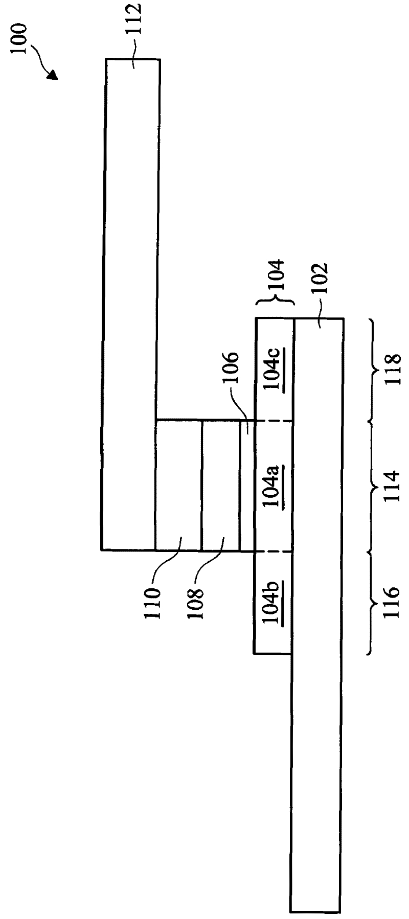
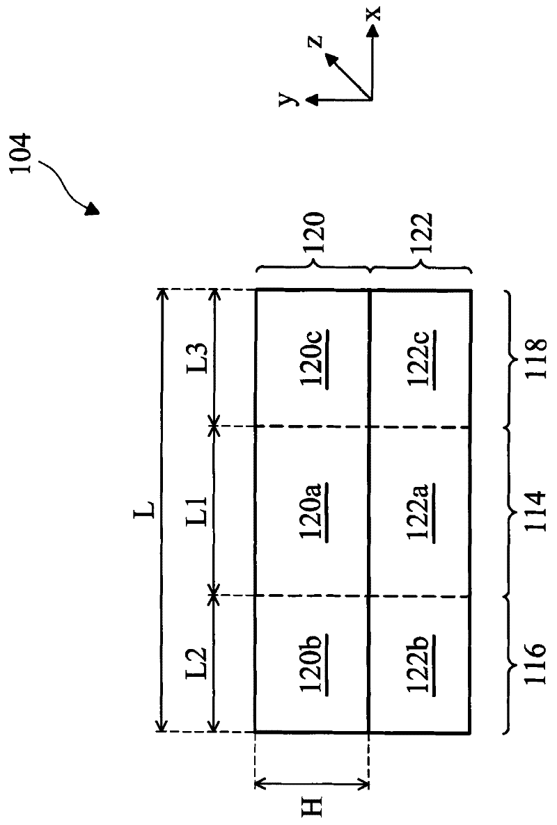
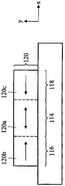
[0080] figure 1 It is a cross-sectional view showing a semiconductor memory device 100 constructed according to an embodiment disclosed in the present invention. Please refer to figure 1 ,this Figure 1 Also, the semiconductor memory element 100 and its manufacturing method will be described. The semiconductor memory device 100 is part of a spin torque transfer magnetic random access memory (STT-MRAM). In one embodiment, the semiconductor memory device 100 includes a stack formed of a plurality of material layers, which functions as a magnetic tunnel junction (MTJ), and according to various disclosed embodiments of the present invention There are different configurations.

[0081] The semiconductor memory device 100 is formed on a semiconductor substrate, such as a silicon substrate or other suitable semiconductor substrates. The semiconductor memory device 100 includes a first electrode (or bottom electrode) 102, wherein the first electrode is formed of a conductive mate...


PUM


Abstract

A semiconductor memory device includes a first ferromagnetic layer magnetically pinned and positioned within a first region of a substrate; a second ferromagnetic layer approximate the first ferromagnetic layer; and a barrier layer interposed between the first ferromagnetic layer and the first portion of the second ferromagnetic layer. The second ferromagnetic layer includes a first portion being magnetically free and positioned within the first region; a second portion magnetically pinned to a first direction and positioned within a second region of the substrate, the second region contacting the first region from a first side; and a third portion magnetically pinned to a second direction and positioned within a third region of the substrate, the third region contacting the first region from a second side. The semiconductor memory device allows written current to be minimized without degrading of magnetoresistance (MR) and\or thermal stability.

Description

technical field [0001] The present invention relates to a semiconductor element, in particular to a semiconductor memory element and its manufacturing method. Background technique [0002] Among semiconductor integrated circuit components, spin torque transfer magnetic random access memory (STT-MRAM) is an emerging technology that can be applied to next-generation embedded memory devices. As densities continue to increase, semiconductor integrated circuit technology continues to advance to enable circuit layouts with smaller feature sizes. However, an excessively large writing current will limit the size of the transistor and result in an excessively large cell size. Therefore, reducing the writing current is a challenging issue for the continuous development of this technology. Some existing methods can reduce the write current, but also reduce the thermal stability of tunnel magnetoresistance (TMR) and spin torque transfer magnetic random access memory (STT-MRAM) devices...

Claims


Application Information

Patent Timeline
Patent Type & Authority Applications(China)
IPC IPC(8): H01L27/22G11C11/16H01L43/08H01L43/12
CPCG11C11/161H01L27/228H01L43/12H01L43/08G11C19/0808G11C11/1675G11C11/1657H10B61/22H10N50/10H10N50/01
Inventor 赖志煌黄胜煌黄国峰刘明德林春荣高雅真陈文正
Owner TAIWAN SEMICON MFG CO LTD
Why Eureka
Try Eureka