Eureka AIR delivers breakthrough ideas for toughest innovation challenges, trusted by R&D personnel around the world.

Plasma processing apparatus and plasma processing method

A plasma and processing device technology, applied in the field of plasma processing, can solve the problems of loss, high RF power, and the reduction of plasma generation efficiency, and achieve the effects of reducing power loss, simplifying the matching device, and improving the generation efficiency

Active Publication Date: 2012-04-18
TOKYO ELECTRON LTD
View PDF10 Cites 19 Cited by
  • Summary
  • Abstract
  • Description
  • Claims
  • Application Information

AI Technical Summary

Problems solved by technology

Therefore, there is a problem that a large RF power loss occurs in the high-frequency power supply unit (especially the matching unit), and the RF power supplied to the plasma load is reduced by this amount, thereby reducing the plasma generation efficiency.

Method used


Image

  • Plasma processing apparatus and plasma processing method
  • Plasma processing apparatus and plasma processing method
  • Plasma processing apparatus and plasma processing method

Examples


other Embodiment approach

[0141] (Other Embodiments or Modifications)

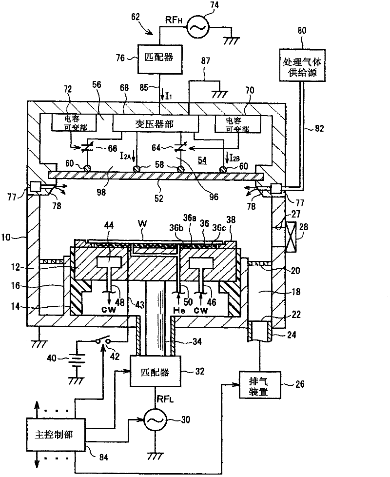
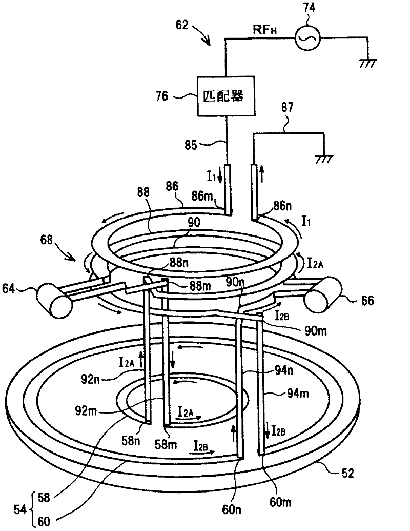
[0142] The inductively coupled plasma processing apparatus of the above-mentioned embodiment ( figure 1 , figure 2 ) The transformer unit 68 is installed in the antenna chamber 56 . However, it is also possible to install the transformer unit 68 outside the antenna housing 56 . In addition, the arrangement posture and direction of the primary coil 86 and / or the secondary coils 88 and 90 can also be selected arbitrarily.

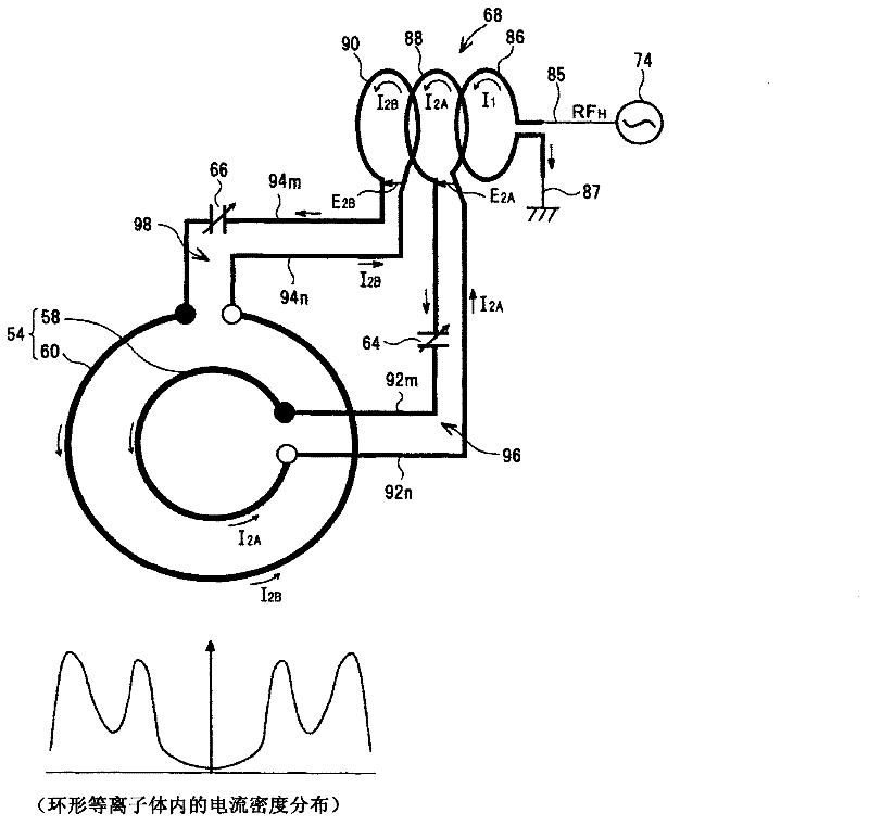
[0143] In the inductively coupled plasma processing apparatus of the above embodiment, capacitors 64 ( 100 ), 66 ( 102 ) are provided in all secondary circuits 96 , 98 formed between coaxial antenna group 54 and transformer unit 68 . However, for example, the primary coil 86 of the transformer unit 68 and the secondary coils 88, 90 each have multiple turns, and a tap changer switch can be attached to the secondary coils 88, 90 (adjustment of the secondary current I by tap changer). 2A , I 2B structure), whil...


PUM


Abstract

There is provided an inductively coupled plasma processing apparatus capable of reducing a RF power loss within a high frequency power supply unit (particularly, a matching unit) and capable of enhancing a plasma generation efficiency. In this inductively coupled plasma processing apparatus, a multiple number of closed-loop secondary circuits 96, 98 independent from each other are formed between a coaxial antenna group 54 and a transformer 68. Further, by varying electrostatic capacitances of variable capacitors 64 and 66, secondary currents I2A and I2B flowing through an inner antenna 58 and an outer antenna 60, respectively, of the coaxial antenna group 54 are independently controlled. Accordingly, it is possible to readily control a plasma density distribution on a semiconductor wafer W in a diametrical direction.

Description

technical field [0001] The present invention relates to the technology of implementing plasma processing on the substrate to be processed, in particular to an inductively coupled plasma processing device and a plasma processing method. Background technique [0002] In processes such as etching, deposition, oxidation, and sputtering in the manufacturing process of semiconductor devices or FPDs (Flat Panel Displays), plasma is often used in order to allow processing gases to react well at relatively low temperatures. Conventionally, plasma generated by high-frequency discharge in the MHz region has been often used for such plasma treatment. Plasma emitted by high-frequency discharge is roughly classified into capacitively coupled plasma and inductively coupled plasma as more specific (device) plasma generating methods. [0003] Generally, an inductively coupled plasma processing apparatus has a dielectric window constituting at least a part of the wall of the processing conta...

Claims


Application Information

Patent Timeline
Patent Type & Authority Applications(China)
IPC IPC(8): H01J37/32H05H1/46
CPCH01J37/3211H01J37/32174H01J37/321H01J37/32183
Inventor 山泽阳平
Owner TOKYO ELECTRON LTD
Why Eureka
Eureka Blog
Learn More