Equipment removal rate monitoring method

A technology of removal rate and equipment, applied in the direction of semiconductor/solid-state device testing/measurement, etc., can solve the problems of prolonged wafer cycle time, high cost and time consumption, and difficulty in recycling and reuse of wafers, so as to increase detection efficiency, improve work efficiency, and prolong the effect of normal production time

Active Publication Date: 2016-12-14
SHANGHAI HUAHONG GRACE SEMICON MFG CORP
View PDF4 Cites 0 Cited by
  • Summary
  • Abstract
  • Description
  • Claims
  • Application Information

AI Technical Summary

Problems solved by technology

However, the use of patterned short-ring wafers as monitoring objects will lead to a substantial increase in production costs. This is because: first, patterned wafers are more difficult to be recycled, or the cost and time consumption of recycling are relatively large; Second, patterned wafers require more preparation time, resulting in longer cycle times for the wafers

Method used


Image

  • Equipment removal rate monitoring method
  • Equipment removal rate monitoring method
  • Equipment removal rate monitoring method

Examples


Embodiment 1

[0036] Embodiment 1: a single layer to be etched, and the etching stops at the stop layer.

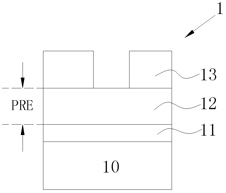
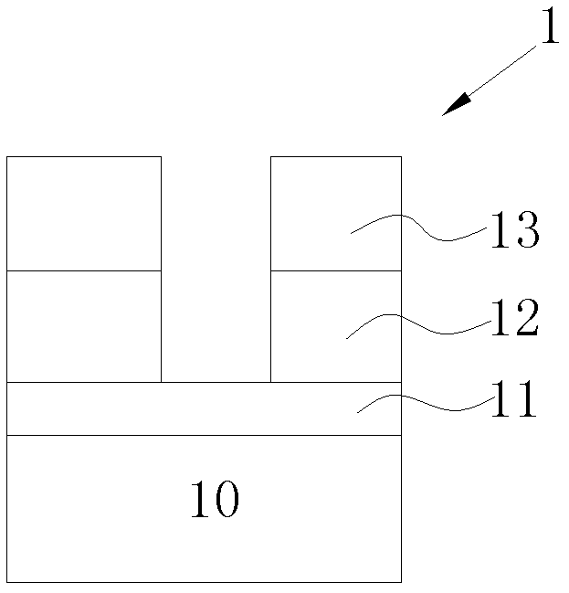
[0037] see Figure 1aThe shown production wafer 1 includes a substrate 10, a stop layer 11 formed on the substrate 10, a layer to be etched 12 formed on the stop layer 11, and a patterned mask layer formed on the layer to be etched 12 13. Wherein, the substrate 10 may be a silicon substrate, a germanium substrate, silicon-on-insulator, or other semiconductor substrates. Described stop layer 11 can be oxide, nitride or oxynitride according to the needs of actual production, certainly, when substrate 10 itself and layer 12 to be etched have large etch selective ratio, also can be the substrate 10. surface. The layer to be etched 12 may be oxide, nitride, oxynitride, polysilicon, etc., and has a large etching selectivity ratio with the stop layer 11, for example, an etching selectivity ratio greater than 10. The patterned mask layer 13 can be a photoresist or other hard mask, and can b...

Embodiment 2

[0039] Embodiment 2: single layer to be etched, etching does not stop at the stop layer.

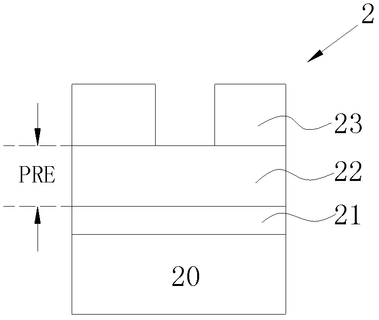
[0040] see Figure 2a Production wafer 2 is shown, with Figure 1a Similarly, it includes a substrate 20 , a stop layer 21 formed on the substrate 20 , a to-be-etched layer 22 formed on the stop layer 21 , and a patterned mask layer 23 formed on the to-be-etched layer 22 .

[0041] Before etching, first measure the thickness PRE of the layer 22 to be etched; then use (dry or wet) etching equipment to etch the layer 22 to be etched exposed by the patterned mask layer 23 in the production wafer 2, and only part of the thickness is to be etched. The etching layer 22 is etched, and the etching stops at the layer 22 to be etched itself, see Figure 2b , while using Advanced Process Control (Advanced Process Control) equipment to monitor the etching process and obtain the time T of the etching process EPD . Measure the remaining thickness POS of the layer to be etched 22 exposed at this tim...

Embodiment 3

[0042] Embodiment 3: Multi-layer composite layer to be etched, etching stops at the stop layer.

[0043] see Figure 3a Production wafer 3 shown, with Figure 1a Similar includes the substrate 30, the stop layer 31 formed on the substrate 30, the to-be-etched layer formed on the stop layer 31 by composite superposition of two or more single layers 321, 322...32n, forming A patterned mask layer 33 on the layer to be etched 321 .

[0044] Before etching, first measure the thickness PRE of each single layer 321, 322...32n in the layer to be etched 1 、PRE 2 ......PRE n ; Then use dry etching equipment to etch each single layer 321, 322 ... 32n exposed by the patterned mask layer 33 in the production wafer 3 in sequence, and at the same time use end point detection equipment to monitor the etching process, And make the etching process of the layer to be etched stop on the stop layer 31, see Figure 3b . The etching time T of each single layer 321, 322...32n is collected from ...


PUM


Abstract

The present invention relates to the technical field of semiconductor manufacturing, in particular to a method for monitoring the removal rate of equipment. The removal rate is obtained by dividing the thickness removal amount of the layer to be removed on the wafer within the predetermined time by the predetermined time, wherein: the The wafer is a production wafer, and the production wafer includes a substrate, a stop layer on the substrate, and a layer to be removed formed on the stop layer. The present invention has the following advantages: first, there is no need to prepare additional removal rate monitoring wafers, which can save costs; second, real-time monitoring can be carried out during wafer production; third, the normal production time of equipment is extended; fourth, increased The detection rate of abnormal removal rate improves the monitoring sensitivity and detects abnormal removal rate early.

Description

technical field [0001] The invention relates to the field of semiconductor manufacturing, in particular to a method for monitoring the removal rate of semiconductor equipment. Background technique [0002] In the field of semiconductor manufacturing, the removal rate of equipment is a very important monitoring index, which can not only be used for monitoring and feedback on the performance of the equipment itself, but also has a great influence on the selection of the end point of the removal process. In most factories, the removal rate of the blanket film layer (Blanket Film) on the wafer surface is used as the monitored object most of the time. However, the detection rate of device removal rate anomalies tends to be low due to differences between the monitor wafers covered with thin film layers and the patterned production wafers. [0003] In general, patterned short loop wafers can also be used as monitoring objects because there are only very small differences compared ...

Claims


Application Information

Patent Timeline
Patent Type & Authority Patents(China)
IPC IPC(8): H01L21/66
Inventor 王百钱奚斐
Owner SHANGHAI HUAHONG GRACE SEMICON MFG CORP
Why Eureka
Try Eureka