Eureka AIR delivers breakthrough ideas for toughest innovation challenges, trusted by R&D personnel around the world.

8-value memory cell embedded in dram storage matrix, and corresponding conversion circuit thereof

A storage unit circuit and storage matrix technology, applied in information storage, static memory, digital storage information, etc., can solve the problems of limited range of control threshold, inability to realize the opening property of MOS transistor threshold interval, complex structure, etc.

Inactive Publication Date: 2012-04-25
HEILONGJIANG UNIV
View PDF2 Cites 12 Cited by
  • Summary
  • Abstract
  • Description
  • Claims
  • Application Information

AI Technical Summary

Problems solved by technology

[0002] With the rapid development of MOS integrated circuit technology, the integration scale is getting larger and higher, and VLSI (Very Large Scale Integration) has some shortcomings: ① First, on the VLSI substrate, the wiring takes up more than 70% of the silicon Chip area; in programmable logic devices (such as FPGA and CPLD), there are also a large number of programmable internal wiring (including programmable connection switches, such as fuse switches, anti-fuse switches, floating gate programming components, etc.), Connect each logic function block or input / output to complete a specific function circuit, wiring (including programming connection switch) accounts for a large cost of materials
[0006] 2. In realizing multi-valued circuits, including realizing binary-multi-valued conversion circuits and multi-valued-binary conversion circuits, prior art control of MOS tube thresholds has great disadvantages: 1. can only control the amplitude of thresholds, and cannot realize The threshold interval of the MOS tube is turned on. If the MOS tube is required to be turned on only when the input is within the specified voltage range, this voltage range is called a band interval, similar to the MOS tube being turned on only when the input is in the high range, and only when the input is in the high range. In the low range, the MOS tube is turned on
Multi-valued logic gates must have a variety of MOS transistors with open properties to make the circuit structure the simplest. However, the current technology that only controls the threshold amplitude makes the structure of multi-valued circuits very different and complicated, which affects its realization.
②The range of the control threshold is limited (because the ion implantation concentration is limited), and the resolution of the turn-on is very low; and the control threshold range in the process often changes the performance of the MOS tube. The adjustment has an influence on the performance and stability of the tube, the stable V tn and V tp Very important
Therefore, the voltage-type multi-valued circuit is not larger than the 4-valued circuit at present, and the application of more-valued circuits is more difficult
③ It is necessary to add an additional process of ion implantation, and the threshold can only be controlled in the semiconductor manufacturing process, which not only increases the complexity of the process, but also cannot be controlled by the user later, or the threshold cannot be programmed by the user

Method used


Image

  • 8-value memory cell embedded in dram storage matrix, and corresponding conversion circuit thereof
  • 8-value memory cell embedded in dram storage matrix, and corresponding conversion circuit thereof
  • 8-value memory cell embedded in dram storage matrix, and corresponding conversion circuit thereof

Examples


Embodiment 1

[0039] Embodiment 1: Description of the functions realized by the 2-8 value conversion circuit BMVC.

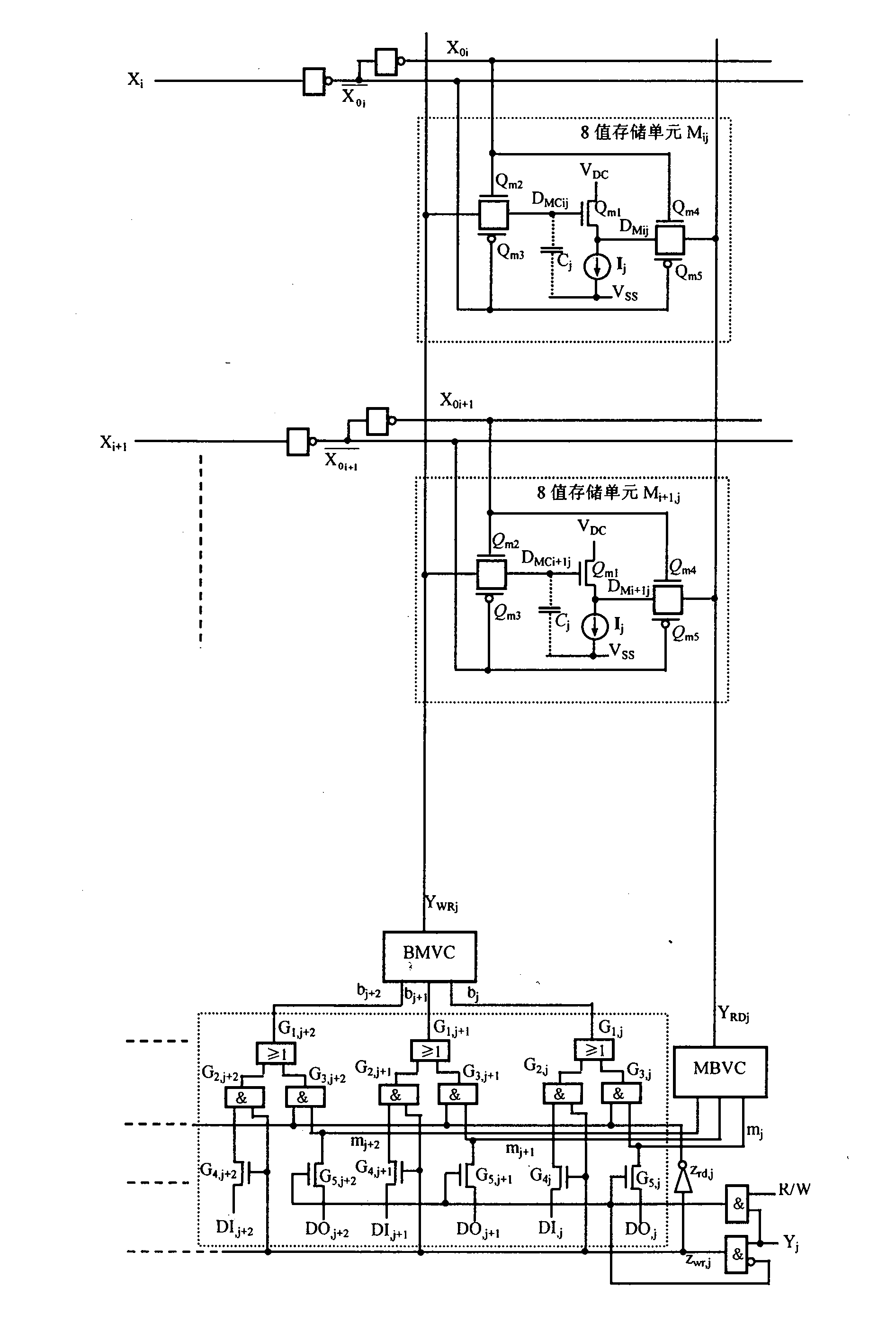
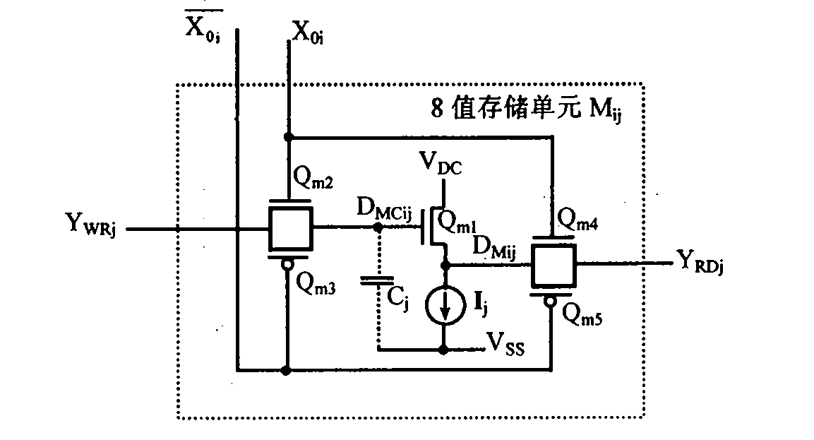
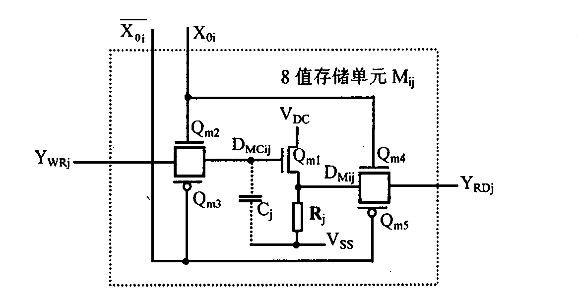
[0040] see Figure 4 ( Figure 1~5 Middle V DC =1.8V, V SS = -3.5V, V D =0V), gate f j7 ~ f j1 (There are two kinds of NAND gate and NOT gate) The working voltage is V DC , gate f j7 ~ f j1 Output high level near V DC , the output low level is close to 0V; ①When b j+2 b j+1 b j =111, f j7 = 0, f j7 Send low level to PMOS tube Q a7 gate, tube Q a7 conduction, V DC directly connected to Y WRj , Y WRj output voltage V YWRj =V DC (logic 7); ② when b j+2 b j+1 b j =110, f j7 = 1 and f j6 = 0, f j7 Send high level to tube Q a7 gate, tube Q a7 cut off, f j6 Send low level to tube Q a6 gate, tube Q a6 conduction, V DC connected to Y through a conduction diode WRj , V YWRj =V DC -V d (logic 6); ③ when b j+2 b j+1 b j =101, f j7 = f j6 = 1 and f j5 = 0, f j7 , f j6 Each sends a high level to the tube Q a7 , Q a6 gate, tube Q a7 , Q a6 cut...

Embodiment 2

[0041] Embodiment 2: Description of the functions realized by the 8-2 value conversion circuit MBVC.

[0042] see Figure 5 , consider the tube G B0mj ~G B3mj The gate of the gate is connected to the input Y through a band-pass-band-resistance variable threshold circuit RDj , tube G H4mj ~G H6mj The gate of the gate is connected to the input Y through the high-pass-low-pass variable threshold circuit RDj , where the tube G H4mj in Y RDj When the input is logic 4~7, it is turned on, and the tube G H5mj in Y RDj When the input is logic 6 and 7, it is turned on, and the tube G H6mj in Y RDj When the input is only logic 7, it is turned on, and the tube G B0mj in Y RDj When the input is only logic 2 and 3, it is turned on, and the tube G B1mj in Y RDj The input is only turned on when the logic level is 1, and the tube G B2mj in Y RDj The input is only turned on when the logic level is 3, and the tube G B3mj in Y RDj The input turns on only at logic level 5, also c...

Embodiment 3

[0043] Example 3: to Figure 3-5 Pspice computer simulation waveform Figures 10-14 instruction of.

[0044] Figure 10The circuit for embedding a 2-value DRAM memory matrix for an 8-value memory cell is in X i and Y j When high level, b j+2 , b j+1 , b j , Y WRj , Y RDj 、m j+2 、m j+1 、m j The waveform diagrams are separated up and down in sequence. It can be seen from the figure that when the input b of BMVC j+2 b j+1 b j =000~111 (the above 3 waveforms), BMVC output Y WRj It is an 8-valued signal 0~8 (the fourth waveform), and the 8-valued signal is obtained by the 8-valued storage unit Y RDj (5th waveform), Y RDj Input to MBVC, and finally MBVC outputs m j+2 m j+1 m j =000~111 (the following 3 waveforms), MBVC has 3-bit 2-value output m j+2 m j+1 m j waveform with BMVC's 3-bit 2-valued input b j+2 b j+1 b j The waveform is the same; Note: X i and Y j The high and low levels are each near V DC and 0; due to TG 1 and TG 2 It is to transmit 8-valu...


PUM


Abstract

The invention discloses an 8-value memory cell embedded in a DRAM storage matrix, and a corresponding conversion circuit thereof. The 8-value memory cell is composed of 3 NMOS tubes, 2 PMOS tubes, a storage capacitor Cj and a power source. An NMOS tube Qm1 and a current source Ij form a source follower FS, wherein a drain of the NMOS tube Qm1 is connected to a direct current power supply VDC, a source electrode of the NMOS tube Qm1 is connected to one terminal of the current source Ij, the other terminal of the current source Ij is connected to a negative direct current power supply VSS, and current from the current source Ij flows from the source electrode of the NMOS tube Qm1 to the negative direct current power supply VSS. A gate electrode of the NMOS tube Qm1 is connected to one terminal of the storage capacitor Cj. The main part of the 8-value memory cell is the NMOS tube source follower. The structure of the 8-value memory cell is simple. With the 8-value memory cell, the characteristics of the DRAM storage matrix are maintained, and BMVC and MBVC are realized. The 8-value memory cell has anti-interference capability and multi-valued information recoverability.

Description

technical field [0001] The invention belongs to the field of digital integrated circuits, in particular to an 8-valued storage unit embedded in a DRAM storage matrix and a related conversion circuit. Background technique [0002] With the rapid development of MOS integrated circuit technology, the integration scale is getting larger and higher, and VLSI (Very Large Scale Integration) has some shortcomings: ① First, on the VLSI substrate, the wiring takes up more than 70% of the silicon Chip area; in programmable logic devices (such as FPGA and CPLD), there are also a large number of programmable internal wiring (including programmable connection switches, such as fuse switches, anti-fuse switches, floating gate programming components, etc.), To connect each logic function block or input / output to complete a specific function circuit, wiring (including programming connection switches) accounts for a large cost of materials. Reducing the proportion of wiring costs becomes a v...

Claims


Application Information

Patent Timeline
Patent Type & Authority Applications(China)
IPC IPC(8): G11C11/4063
Inventor 方振贤刘莹方倩
Owner HEILONGJIANG UNIV
Why Eureka
Eureka Blog
Learn More