Any k-value and 8-value dram storage unit and writing and reading circuit

A storage unit circuit and a writing circuit technology are applied in the fields of storage unit circuits, writing circuits and reading circuits, and can solve the problems of complex structure, inability to control the threshold value by the user later, and different threshold voltage turn-on properties.

Inactive Publication Date: 2011-12-21
HEILONGJIANG UNIV
View PDF3 Cites 3 Cited by
  • Summary
  • Abstract
  • Description
  • Claims
  • Application Information

AI Technical Summary

Problems solved by technology

[0002] With the rapid development of MOS integrated circuit technology, the integration scale is getting larger and higher, and VLSI (Very Large Scale Integration) has some shortcomings: ① First, on the VLSI substrate, the wiring takes up more than 70% of the silicon Chip area; in programmable logic devices (such as FPGA and CPLD), there are also a large number of programmable internal wiring (including programmable connection switches, such as fuse switches, anti-fuse switches, floating gate programming components, etc.), Connect each logic function block or input/output to complete a specific function circuit, wiring (including programming connection switch) accounts for a large cost of materials
[0006] 2. In the realization of multi-valued circuits, the existing technology to control the threshold of MOS transistors has great disadvantages: ① the amplitude of the control threshold is limited (because the ion implantation concentration is limited), and the resolution of opening is low; and the amplitude of the control threshold in the process is often Change the performance of the MOS tube, for example, the decrease of the threshold voltage will lead to a sharp increase of the cut-off current, the adjustment of the threshold voltage will affect the perfor

Method used


Image

  • Any k-value and 8-value dram storage unit and writing and reading circuit
  • Any k-value and 8-value dram storage unit and writing and reading circuit
  • Any k-value and 8-value dram storage unit and writing and reading circuit

Examples


Embodiment 1

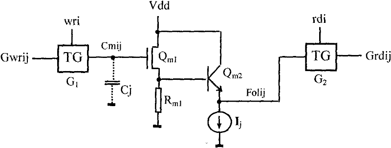
[0043] Embodiment 1: Description of the circuit information function of the storage unit.

[0044] The storage unit circuit has three information functions of multi-value information storage, multi-value information reception and multi-value information sending: ①Information reception: by figure 1 It can be seen that the write pulse w ri When coming, the transfer gate G 1 conduction, will write the bit line G wrij The multi-valued information is transferred to the storage capacitor C j , so that the capacitor C j Receive multi-valued information C mij ; Capacitance C j Reception is a charging and discharging process, whether charging or discharging depends on the capacitance C j The original stored information and the current received information, the charging and discharging time constant is C j Capacitance related, C j Usually only a few picofarads, no larger; ②Information storage: write pulse w ri When the future arrives, the transmission gate G 1due by figure 1 ...

Embodiment 2

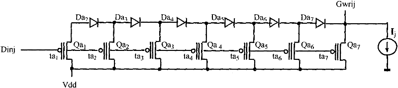
[0048] Embodiment 2: Proof that the writing circuit of arbitrary K value and 8-value DRAM satisfies design requirements.

[0049] The writing circuit of any K value DRAM is shown as Figure 4 , it is necessary to prove that the design requirements are met: when writing into the circuit input D inj When the logic value is 0, 1, 2, 3, 4, ..., L-2, L-1, L, the write circuit outputs G wrij Logical values ​​are still sequentially 0, 1, 2, 3, 4, ..., L-2, L-1, L; but G wrij Logical value corresponds to logic level V Gwrij (n) than D except 0 level inj Logical value corresponds to logic level V Dinj (n) High Δ (n=1~L), the 0 level is still 0, that is, V Gwrij (0)=V Dinj (0) = 0V, V Gwrij (1) = V Dinj (1)+Δ, V Gwrij (2) = V Dinj (2)+Δ,...,V Gwrij (L-1)=V Dinj (L-1)+Δ, V Gwrij (L)=V Dinj (L)+Δ,V Dinj (k)>V Dinj (k-1); ta k Adjacent logic level V for the write circuit input Dinj (k) and V Dinj The middle value of (k-1), satisfying V Dinj (k-1)k Dinj (k), k=1, 2, 3, 4...

Embodiment 3

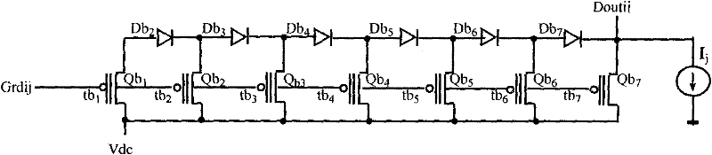
[0052] Embodiment 3: Proof that the readout circuit of any K value and 8-value DRAM satisfies the design requirements.

[0053] The readout circuit of any K value DRAM is shown as Figure 5 , it is necessary to prove that the design requirements are satisfied: when the input G of the readout circuit rdij When the logic value is 0, 1, 2, 3, 4, ..., L-2, L-1, L, the input D of the readout circuit outj Logical values ​​are still sequentially 0, 1, 2, 3, 4, ..., L-2, L-1, L; G rdij ,D inj and D outj The logic value corresponds to the logic level in order of V Grdij (n), V Dinj (n) and V Doutj (n)(n=0~L), where input G rdij It is a non-standard K value signal, and it is required to output D outj is the standard equal-step K value signal, that is, V Doutj (0)=V Dinj (0) = 0V, V Doutj (1) = V Dinj (1) = V Don , V Doutj (2) = V Dinj (2) = 2V Don , V Doutj (3) = V Dinj (3) = 3V Don ,... V Doutj (L-2)=V Dinj (L-2)=(L-2)V Don , V Doutj (L-1)=V Dinj (L-1)=(L-1)V D...


PUM


Abstract

The invention discloses a storage unit circuit, a write circuit and a read circuit for any K-valued and 8-valued DRAM (dynamic random access memory). The storage unit circuit comprises a voltage follower (F), a storage capacitor (Cj) of the grid of the voltage follower (F), a CMOS (complementary metal oxide semiconductor) transmission gate (G1) and a CMOS transmission gate (G2); in consideration of the direct-current level offset (Delta) between the input and output of the voltage follower (F), the write circuit is so designed that a multi-valued signal which is direct-current level offset (Delta) higher than the input of the write circuit can be provided; and in addition, since the voltage amplification factor of the voltage follower (F) is less than 1, the output waveform of the voltage follower (F) is smaller than the input waveform or is unequi-stepped, and the read circuit is designed for correction, the non-regular multi-valued signal is converted into a regular (equi-stepped) multi-valued signal. Both the write circuit and the read circuit have a good quantitative shaping effect, the original multi-valued information can be easily recovered when the voltage change of the storage capacitor (Cj) does not exceed a maximum new threshold and a minimum new threshold, and therefore the invention has anti-interference capability and multi-valued information-recovering capability. The invention is mainly used in the technical fields of VLSIs (very large-scale integrated circuit), such as FPGAs (field programmable gate array), CPLDs (complex programmable logic device), semi-custom or full-custom ASICs (application specific integrated circuit) and memories, and other digital ICs (integrated circuit).

Description

(1) Technical field [0001] The invention belongs to the field of digital integrated circuits, in particular to a storage unit circuit, a writing circuit and a reading circuit of an arbitrary K value and 8-value DRAM. (2) Technical background [0002] With the rapid development of MOS integrated circuit technology, the integration scale is getting larger and higher, and VLSI (Very Large Scale Integration) has some shortcomings: ① First, on the VLSI substrate, the wiring takes up more than 70% of the silicon Chip area; in programmable logic devices (such as FPGA and CPLD), there are also a large number of programmable internal wiring (including programmable connection switches, such as fuse switches, anti-fuse switches, floating gate programming components, etc.), To connect each logic function block or input / output to complete a specific function circuit, wiring (including programming connection switches) accounts for a large cost of materials. Reducing the proportion of wir...

Claims


Application Information

Patent Timeline
IPC IPC(8): G11C11/4096
Inventor 方振贤刘莹
Owner HEILONGJIANG UNIV
Why Eureka
Try Eureka